Elucidation of crystal and electronic structures within highly strained bifeo3 by transmission electron microscopy and first-principles simulation
- Select a language for the TTS:
- UK English Female
- UK English Male
- US English Female
- US English Male
- Australian Female
- Australian Male
- Language selected: (auto detect) - EN
Play all audios:
ABSTRACT Crystal and electronic structures of ~380 nm BiFeO3 film grown on LaAlO3 substrate are comprehensively studied using advanced transmission electron microscopy (TEM) technique
combined with first-principles theory. Cross-sectional TEM images reveal the BiFeO3 film consists of two zones with different crystal structures. While zone II turns out to have rhombohedral
BiFeO3, the crystal structure of zone I matches none of BiFeO3 phases reported experimentally or predicted theoretically. Detailed electron diffraction analysis combined with
first-principles calculation allows us to determine that zone I displays an orthorhombic-like monoclinic structure with space group of _Cm_ (=8). The growth mechanism and electronic
structure in zone I are further discussed in comparison with those of zone II. This study is the first to provide an experimentally validated complete crystallographic detail of a highly
strained BiFeO3 that includes the lattice parameter as well as the basis atom locations in the unit cell. SIMILAR CONTENT BEING VIEWED BY OTHERS LARGE BI-AXIAL TENSILE STRAIN EFFECT IN
EPITAXIAL BIFEO3 FILM GROWN ON SINGLE CRYSTAL PRSCO3 Article Open access 03 November 2023 FOUR DIMENSIONAL-SCANNING TRANSMISSION ELECTRON MICROSCOPY STUDY ON RELATIONSHIP BETWEEN
CRYSTALLOGRAPHIC ORIENTATION AND SPONTANEOUS POLARIZATION IN EPITAXIAL BIFEO3 Article Open access 05 July 2024 STRUCTURAL PROPERTIES OF BI THIN FILM GROWN ON SI (111) BY QUASI-VAN DER WAALS
EPITAXY Article Open access 17 February 2022 INTRODUCTION BiFeO3 (BFO) has been known as a multiferroic material with ferroelectricity and essentially _G_-type antiferromagnetism1,2, which
has application potential for emerging spintronics technology such as multiple-state memory and magnetic random access memory. While its magnetoelectric response was found too weak for
practical device application1,3 in the past, recent studies using high quality single crystalline bulk BFO4,5 have revealed the true polarization value is one order of magnitude higher than
previous thought, i.e., ~60 μC cm−2. Besides, with the availability of high quality single crystalline oxide substrates, BFO thin films grown epitaxially have shown significantly increased
polarization values around 90–115 μC cm−2 6,7,8,9. Since the crystal structure and/or lattice parameters of the substrates are different from those of BFO material, BFO thin films are
expected to be under lattice stress/strain, which is closely related to increased polarization values as well as other physical properties in epitaxial BFO thin films. Thus, considerable
experimental and theoretical efforts have been devoted to understand the lattice stress/strain effects on epitaxial BFO films that present lattice distortions found in rhombohedral unit cell
of bulk BFO6,10,11,12 and also different BFO crystal unit cell structures13,14,15,16,17,18,19,20. Recently, it was suggested that, while BFO thin films are likely to possess tetragonal
and/or monoclinic structures (denoted as M_C_ and M_A_) under compressive stress, they rather grow as orthorhombic and/or monoclinic structures of a different type (M_B_) under tensile
stress21. However, the precise crystal models that can explain experimentally found highly stressed BFO are rather unclear as has been pointed out very recently22,23. Most of the
experimental reports dealing with strain effects on epitaxially grown BFO films are making discussions based on lattice parameter changes and/or unit cell
distortion6,10,11,12,13,14,15,16,17,18,19,20. On the other hand, it is worth noting that when those lattice parameter changes and/or unit cell distortions occur in epitaxially grown BFO
films, _locations of basis atoms_ in the unit cell change as well, which lead to corresponding alteration in its reciprocal space in terms of locations, symmetries, and shapes in Bragg’s
reflections. In particular, for a material like BFO consisting of multiple elements, the alteration in the reciprocal space can be more dramatic in that slight changes in the location of
each constituent atom can readily cause extra Bragg’s reflections. In order to address this challenging issue adequately, a careful investigation on wide range reciprocal space information,
i.e., _Q_ (scattering vector) of >200 nm−1, is required to be compared with structure factor calculation results of possible crystal models (either simulated by first-principles theory or
derived by powder x-ray diffraction technique) that provide not only lattice parameter but also _locations of all the basis atoms_ in the unit cell. To the best of our knowledge, no
previous experimental reports have discussed about this except for those dealing with bulk BFO crystal structure24,25. In this study, a comprehensive approach combining aberration-corrected
transmission electron microscopy (TEM) and first-principles methods has been utilized to unveil a complete crystal structure that includes lattice parameter as well as locations of basis
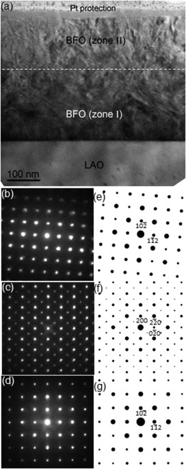
atoms in the unit cell. In addition, growth behavior of a highly strained BFO thin film grown on LaAlO3 (LAO) is discussed as well. RESULTS AND DISCUSSION Figure 1(a) shows a cross-sectional
bright-field (BF) TEM image of the BFO films grown on LAO substrate along the [241] zone axis. It exhibits two distinctive layers with darker and brighter contrasts denoted as zone I and
zone II, respectively. In addition, both of the zones show contrasts associated with lattice defects and lattice stress. In order to acquire information about crystallographic details on the
two zones, electron diffraction (ED) patterns were recorded from both of them using ~80 nm diameter of electron probe, as shown in Fig. 1(b) and (c). The boundary between zones I and II are
drawn ~200 nm above zone I/LAO interface based on the ED analysis making use of ~3 nm diameter of electron probe. Note that the true boundary morphology might not be perfectly straight in
atomistic scale. It will be discussed later with atomic resolution images. The ED pattern from the [241] zone axis of the LAO substrate is also obtained, as shown in Fig. 1(d), to use it as
an undistorted reference material for precise camera length calibration. Note that symmetry of the Bragg’s reflections in the ED pattern from zone II (Fig. 1(b)) is identical to that in the
ED pattern from LAO substrate (Fig. 1(d)), indicating that the crystal structure of BFO in zone II is rhombohedral, i.e., that of bulk BFO. Note that the orientation of Bragg’s reflection
along the surface normal direction in Fig. 1(b) is ~4° off from that in Fig. 1(d). The reason will be discussed later with a high resolution TEM image. On the other hand, the ED pattern from
zone I (Fig. 1(c)) is obviously different from that of zone II in terms of its symmetry as well as the locations of Bragg’s reflections, indicating a different crystal structure. As
discussed in previous reports24,25, it is necessary to perform an ED analysis from another zone axis to confirm its crystal structure correctly since an ED pattern obtained from TEM is
merely a two dimensional cross-section of the three dimensional reciprocal lattice of the material. Thus, the same sample was prepared for TEM observation along [211] zone axis, i. e., 45°
away from [241], of LAO substrate as shown in Fig. 2. Figure 2(a) shows a BF TEM image with zones I and II whose characteristics are the same as those in Fig. 1(a). The ED patterns recorded
from zone II, zone I and the LAO substrate with an electron probe of ~80 nm diameter are shown in Fig. 2(b,c) and (d), respectively. Similarly to Fig. 1, we find that, while the ED pattern
from zone II (Fig. 2(b)) is the same as that from LAO substrate (Fig. 2(d)) in terms of symmetry in Bragg’s reflections, zone I is distinctively different in terms of symmetry as well as
locations of Bragg’s reflections. Note that the orientations of all the ED patterns are preserved with respect to the BF images in Figs 1 and 2 to further investigate the epitaxial
relationships among zone I, zone II and the LAO substrate. For a precise ED pattern analysis, the structure factor, _F__hkl_, where _hkl_ represents a specific Bragg’s reflection, was
calculated for all BFO phases discussed in previous reports (including theoretically predicted metastable ones) that provide all the necessary crystallographic information, including basis
atom locations in the unit cell. These structures are: rhombohedral BFO (space group: _R3c, a_ = 0.5678 nm, _c_ = 1.3982 nm, _α_ = _β_ = 90°, _γ_ = 120°)18, monoclinic BFO (space group:
_P2__1__/m, a_ = 0.5615 nm, _b_ = 0.7973 nm, _c_ = 0.5647 nm, _α_ = 90°, _β_ = 90°, _γ_ = 90.1°)19, tetragonal BFO (space group: _P4mm, a_ = 0.367 nm, _c_ = 0.464 nm)17, monoclinic BFO
(space group: _Pc, a_ = 0.7291 nm, _b_ = 0.5291 nm, _c_ = 0.5315 nm, _α_ = 90°, _β_ = 139.46°, _γ_ = 90°)20, monoclinic BFO (space group: _Cm, a_ = 0.9354 nm, _b_ = 0.7380 nm, _c_ = 0.3804
nm, _α_ = 90°, _β_ = 86.60°, _γ_ = 90°)20, orthorhombic BFO (space group: _Pna2__1_, _a_ = b = 0.5314 nm, _c_ = 0.9452 nm, _α_ = _β_ = _γ_ = 90°)20, monoclinic BFO (space group: _Cc, a_ =
1.0604 nm, _b_ = 0.5322 nm, _c_ = 0.5323 nm, _α_ = 90°, _β_ = 62.80°, _γ_ = 90°)20, orthorhombic BFO (space group: _Pnma, a_ = 0.5650 nm, b = 0.7770 nm, _c_ = 0.5421 nm, _α_ = _β_ = _γ_ =
90°)20, and orthorhombic BFO (space group: _Pna2__1_, _a_ = 0.5702 nm, b = 0.5507 nm, _c_ = 0.8036 nm, _α_ = _β_ = _γ_ = 90°)20. The structure factor for LAO (space group: _R__c, a_ = 0.5366
nm, _c_ = 1.3110 nm, _α_ = _β_ = 90°, _γ_ = 120°) was also calculated to investigate the epitaxial relationship between LAO and BFO overlayers26. The calculation of the ED patterns was
based on kinematical approximation: where _f__n_ is the atomic scattering factor for atom _n_ at fractional coordinates (_x__n_, _y__n_, _z__n_). Details about this type of ED pattern
analysis and structure factor calculation have been given elsewhere24. As a result, it was found that Figs 1(b) and 2(b) correspond to [241] and [211] net patterns of rhombohedral- (_r_-)
BFO, confirming that zone II consists of BFO material with its _bulk crystal structure_. Note that the Bragg’s reflections marked with white arrows in Fig. 2(b) result from double
diffraction24,25. While the ED patterns in Fig. 1(b) and (d) show a four-fold symmetry, they should not be confused with the [100] net pattern of cubic materials, as discussed
previously24,25. It is worth noting that no evidence of significant distortion in BFO rhombohedral lattice was found from Figs 1(b) and 2(b). On the other hand, for Figs 1(c) and 2(c), i.e.,
for the ED patterns from zone I, while none of the aforementioned BFO phases was able to reproduce ED patterns that perfectly match both of Figs 1(c) and 2(c), the [001] net pattern from
the monoclinic BFO from reference 20 (space group: _Cm, a_ = 0.9354 nm, _b_ = 0.7380 nm, _c_ = 0.3804 nm, _α_ = 90°, _β_ = 86.60°, _γ_ = 90°) interestingly match Fig. 1(b) as shown in
supplementary Fig. S1(a). However, none of its net patterns match Fig. 2(c) including the [012] net pattern of which symmetry and Bragg’s reflection locations are similar but different (see
supplementary Fig. S1(b)). It implies the true crystal structure in zone I could be a derivative of it. In fact, a previous study of pulsed laser deposition-grown BFO thin films on LAO
showed that an ED pattern from a local BFO area matches [001] of the _Cm_ phase22. However, no further ED study from another zone axis was performed to confirm the validity of the _Cm_
phase. In order to further explore the crystal structure of zone I, first-principles calculations were performed focusing on the above mentioned _Cm_ phase of BFO. First, we considered the
fixed in-plane lattice parameters of A = (2aIP, 0, 0) and B = (δ’, 2aIP, 0). Here, aIP is the in-plane lattice constant of the LAO substrate (~3.79 Å), and δ’ is about −0.013 Å. This is to
mimic the non-90-degree angle of LAO’s in-plane lattice vectors (~90.1°). Then, we fully optimized the out-of-plane lattice vectors of _Cm_ BFO, which is shown as C = (δ1, δ2, 2aIP+δ3), as
well as the atomic positions. This case is denoted as case (1) in our theoretical study. Note that, here, all δ1, δ2 and δ3 are optimized. Furthermore, we also simulated the _Cm_ phase of
BFO on the LAO substrate by fixing the in-plane lattice vectors (of the _Cm_ phase) as A = (2aIP, 0, 0) and B = (0, 2aIP, 0). Note that here we maintained the angle between two in-plane
lattice vectors as 90° (which is rather close to such angle of LAO substrate, ~90.1°), to mimic a square substrate. Then, we optimize the out of plane lattice vectors of _Cm_ BFO C = (δ1,
δ2, 2aIP+δ3) considering two strategies: (i) optimizing all δ1, δ2 and δ3, and (ii) fixing δ1 and δ2 as 0 and optimizing only δ3. The latter strategy corresponds to the limit of thin films
in which the out-of-plane lattice vector is forced to be perpendicular to the substrate. Strategies (i) and (ii) are denoted cases (2) and (3), respectively, in addition to the above
mentioned case (1). These three cases will allow us to fully compare the experimental TEM images with simulation results for the _Cm_ phase. Structure factor calculations for all three
cases, followed by careful comparison with the ED patterns, lead to a conclusion that only _case_ (3) reproduces a _Cm_ phase that immaculately explains Figs 1(c) and 2(c). The
crystallographic details of the _Cm_ phase are shown in Table 1. (Note that although symmetry of basis atom locations in the unit cell has monoclinic, i.e., _Cm, α, β_ and _γ_ angles are
~90°. Thus, hereafter the _Cm_ BFO phase shown in Table 1 is termed as orthorhombic-like monoclinic.) For example, the ED patterns in Figs 1(c) and 2(c) turned out to match [001] and [012]
net patterns of the _Cm_ phase in Table 1 in terms of symmetry and locations of Bragg’s reflections, as revealed in their corresponding structure factor calculations shown in Figs 1(f) and
2(f), respectively. This suggests that the first-principles approach adopted in the present study successfully generates the crystal structure of BFO in zone I. Based on the results shown in
Figs 1 and 2, the epitaxial relationship between zone I – i.e., _Cm_ BFO, denoted as _m_-BFO hereafter – and the LAO substrate is confirmed as follows: In order to further confirm the
validity of _m_-BFO model, the [241]LAO cross-sectional TEM sample was tilted by ~18° within the TEM column to record the ED patterns from zone I and the LAO substrate, as shown in Fig. 3(a)
and (b), respectively. Structure factor calculations shown in Fig. 3(c) and (d) clearly reveal that they correspond to [016] net pattern of the _Cm_ phase and the [271] net pattern of LAO.
Note that the intensity maxima resulting from double diffraction are denoted with arrows in Fig. 3(b). It is worth noting that the angle between [106] (Fig. 3(a)) and [001] (Fig. 1(c)) of
the orthorhombic-like monoclinic phase is calculated to be 18.4°, which is in good agreement with the angle of 17.9° obtained between [271] (Fig. 3(b)) and [241] (Fig. 1(d)) of the
underlying LAO substrate. This further confirms the validity of the orthorhombic-like monoclinic structure given in Table 1. For comparison, the [016] net pattern of the monoclinic BFO from
reference 20 is calculated as shown in supplementary Fig. S1(c). At first glance, Fig. S1(c) seems similar, but it does not match Fig. 3(a) in terms of: (1) the angle between (200) and (06)
not being 90° and (2) locations of (21) and (01) being different from those in Fig. 3(a). In addition, x-ray diffraction (XRD) with _θ_ − 2_θ_ geometry, i.e., scanning along surface normal
direction, is performed using Cu _Kα_ to investigate the homogeneity of phases throughout the BFO layer as well as possible incorporation of second phases such as Bi2Fe4O9 and Bi2O3 (see
supplemental Fig. S2). As a result, Bragg’s reflections corresponding to surface normal direction from of _m_-BFO and _r_-BFO are confirmed. Note that no Bragg’s peaks are left unexplained.
This is in good agreement with the ED analyses shown in Figs 1, 2 and 3, indicating that the BFO layer is highly homogeneous consisting of _m_-BFO and _r_-BFO only with no second phase
incorporation. To provide more direct information about atomistic structural details, high-angle annular dark-field (HAADF)-scanning TEM (STEM) images were obtained from the interfaces
between zone I (_m_-BFO) and zone II (_r_-BFO) along the [241]LAO zone axis, as shown in Fig. 4. Figure 4(a) shows an area of lattice distortion in zone I, as denoted by a dashed square
indicating that zone I is under lattice strain. Two fast Fourier transform (FFT) patterns shown as insets reveal the same characteristics, i.e., extra columns of Bragg’s reflections in
_m_-BFO only, found in their respective ED patterns (Fig. 1(b) and (c)) confirming that these are not charge coupled device (CCD) camera artifacts nor reflections from higher order Laue
zone, but originate from the BFO crystal structure. It is worth noting that (10) of _r_-BFO is ~3° off the surface normal direction, which is consistent with the angle of ~4° off found in
Fig. 1(b). The reason for this slight tilt angle is considered to be associated with a coherent lattice planes transition at the _m_-BFO/_r_-BFO interface as denoted by arrows in Fig. 4(a).
A magnified HAADF-STEM image from _m_-BFO area is shown in Fig. 4(b) with its atomistic model superimposed. While the locations of the Bi and Fe atoms match their presumed location based on
the atomistic model, it is hard to locate O atoms primarily due to the much lighter atomic mass contrast of oxygen27. Nonetheless, it can be readily concluded that first-principles
calculation, XRD, ED patterns, and structure factor calculation, combined with atomic resolution HAADF verify that BFO in zone I has the orthorhombic-like monoclinic crystal structure
detailed in Table 1. In order to further study the _m_-BFO growth mechanism on LAO substrate, an atomic resolution HAADF-STEM image along the [241]LAO zone axis was acquired from the
_m_-BFO/LAO interface as shown in Fig. 5. It can be readily noticed that lattice planes run smoothly from LAO through _m_-BFO, indicating a _coherent_ interface. In fact, if atomistic models
between _m_-BFO and the LAO substrate are constructed based on the epitaxial relationship found above, as shown in Fig. 6, it can be noticed that the lattice spacings along in-plane
direction between LAO, i.e., (12) with 0.379 nm, and _m_-BFO, i.e., with 0.379 nm match with 0.0% of lattice mismatch along the [241]LAO zone axis (see Fig. 6(a)). Similarly, when projected
along the [211]LAO zone axis (Fig. 6(b)) the lattice spacing match with 0.0% of lattice mismatch along the in plane direction as well. On the other hand, the lattice mismatch between _r_-BFO
and LAO along the in plane direction is, for instance, 5.3% when calculated for of _r_-BFO and of LAO. Thus, it is believed that the minimal lattice mismatch attributed to the epitaxial
relationship found between _m_-BFO and LAO is the reason that _m_-BFO, rather than _r_-BFO, starts to grow on the surface of LAO. As the _m_-BFO layer becomes thicker, however, the biaxial
constraint imposed by LAO substrate should weaken. Thus, the equilibrium BFO phase, i.e., _r_-BFO, is expected to start growing on top of _m_-BFO. Since BFO in zone I is confirmed a new BFO
phase with space group of _Cm_, it is worth investigating its local electronic structure in comparison with that of _r_-BFO using O _K_-edge that is sensitive to local bonding and geometry.
Figure 7 shows the O _K_-edge electron energy loss (EEL) spectra acquired from _r_-BFO, zone II, (a) and _m_-BFO, zone I, (b) with ~1.0 eV energy resolution. It is known that the O _K_-edge
spectrum of BFO is divided in two regions, i.e., a pre-edge region ranging from ~530 to ~538 eV and a post-edge region ranging from ~538 to ~548 eV28,29. For the pre-edge region, the peaks
denoted A in Fig. 7(a) and (b) are attributed to hybridization between O 2_p_ and Fe 3_d_ states28,29. Besides, the shoulders denoted A’ in Fig. 7(a) and (b) are considered to stem from a
transition between O 2_p_ and Bi 5_d_ states or possibly that between O 2_p_ and Bi 6_d_ states in BFO28,29,30. On the other hand, the (sub)peaks denoted B and B’ within the post-edge region
in Fig. 7(a) and (b) are known to be associated with hybridization between O 2_p_ and Fe 4_sp_ states. It has been found that the (sub)peaks split with 1.8~2.0 eV separation for bulk and
thin film BFO using near edge x-ray absorption fine structure technique and electron energy loss spectroscopy28,29,31. While there is no significant difference found within the pre-edge
region between Fig. 7(a) and (b) (except for slightly higher A’/A intensity ratio for _m_-BFO, which is commonly found in BFO thin films28,29,30), a significant difference is found for the
B’/B intensity ratio in the post-edge region between Fig. 7(a) and (b); indeed, while B’ intensity is higher than B in Fig. 7(a), it is much lower than B in Fig. 7(b). This indicates a
substantial difference in the Fe-O bonding states resulting from different coordination geometries for the Fe atoms in _r_-BFO and _m_-BFO. Note that the aforementioned characteristics for
_r_-BFO matches those reported previously for bulk28 and thin film _r_-BFO25 in which Fe atom has octahedron bonding geometry with nearest O neighbors as shown in Fig. 8(a). On the other
hand, the octahedron bonding geometry between Fe and O atoms changes to a pyramidal one in _m_-BFO, as shown in Fig. 8(b). This is considered to be the reason for the dramatically different
B’/B ratios between Fig. 7(a) and (b). Our results are, thus, consistent with previous EEL spectroscopy studies of monoclinic22,31, and pseudotetragonal29 phases from pulsed laser
deposition-grown BFO thin films. SUMMARY In summary, crystal and electronic structures of a ~380 nm BFO film grown on a LAO substrate were studied using advanced TEM techniques and the
first-principles calculations. BF TEM images reveal that the BFO film consists of two zones, i.e., zone I (=_m_-BFO) and zone II (=_r_-BFO), with different crystal structures. Multiple zone
axes ED analysis combined with structure factor calculation readily reveal that crystal structure in zone II is rhombohedral. In contrast, resolving the structure of zone I requires the aid
of first-principles calculations to unveil a new orthorhombic-like monoclinic phase with space group of _Cm_ (=8). The atomic resolution HAADF image at the interface between LAO and zone I
(=_m_-BFO) show a coherent interface with no sign of significant lattice distortion. Atomistic models constructed based on the epitaxial relationship found by ED and structure factor
analysis reveal that the lattice mismatch at the interface between _m_-BFO and LAO substrate is ~0.0%, indicating that _m_-BFO, rather than _r_-BFO grows, on LAO since _m_-BFO can more
efficiently minimize lattice mismatch with LAO. While the O _K_-edge EEL spectrum from _r_-BFO is consistent with that from bulk BFO, that from _m_-BFO shows drastic differences in the
post-edge region, which is considered to be associated with the peculiar bonding geometry, i.e., pyramidal, between iron and oxygen atoms in _m_-BFO. METHODS A BFO thin film was grown on a
(100) LAO substrate to a thickness of ~380 nm using ultrahigh vacuum (<2 × 10⁻⁶ Pa) rf magnetron sputtering at 550 °C. Cross-sectional samples for TEM analysis were prepared by dual beam
focused ion beam technique, FEI Nova 600, followed by low energy ion polishing, Fischione 1040 Nanomill, with 0.5 kV of Ar ion to minimize beam damage effect. Two different TEM systems
operated at 200 kV acceleration voltage were implemented: (1) a JEOL JEM-2100F equipped with Gatan Orius 833 CCD camera for BF TEM images and ED patterns (located in Analytical and
Diagnostics Laboratory at State University of New York at Binghamton) and (2) a FEI Titan2 G2 80–200 electron probe aberration-corrected scanning transmission electron microscope equipped
with Gatan Enfinium spectrometer used to record HAADF-STEM images and EEL spectra (located in ER-C, Forchungszentrum Jülich, Germany). For the first-principles calculations, we used density
functional theory as implemented in the VASP code32,33. For the _Cm_ phase of BFO, the C-type magnetic ordering for Fe spins is considered in our calculations, following the usual approach
that was followed, e.g., in ref. 20. All our simulations were done for a 40-atom supercell that can be viewed as a 2 × 2 × 2 repetition of the elemental 5-atom perovskite unit. The energy
cut-off and k-point mesh were selected as 500 eV and (4, 4, 4), respectively. The PBEsol34 PAW potentials were used in the calculations, with the electronic configurations of
5_d_106_s_26_p_3 for Bi, 3_s_23_p_63_d_74_s_1 for Fe, and 2_s_22_p_4 for O, respectively. A “Hubbard U” correction was used for a better treatment of iron’s 3_d_ electrons35, with the
effective Hubbard U value of 4.0 eV. The crystal structures are relaxed until the force on each atom is less than 0.005 eV/Å. ADDITIONAL INFORMATION HOW TO CITE THIS ARTICLE: Bae, I.-T. _et
al_. Elucidation of crystal and electronic structures within highly strained BiFeO3 by transmission electron microscopy and first-principles simulation. _Sci. Rep._ 7, 46498; doi:
10.1038/srep46498 (2017). PUBLISHER'S NOTE: Springer Nature remains neutral with regard to jurisdictional claims in published maps and institutional affiliations. REFERENCES *
Smolenskii, G. A. & Chupis, I. E. Ferroelectromagnets. _Usp. Fiz. Nauk._ 137, 415–448 (1982). Article CAS Google Scholar * Kiselev, S. V., Ozerov, R. P. & Zhdanov, G. S. Detection
of magnetic order in ferroelectric BiFeO3 by neutron diffraction. _Sov. Phys. Dokl_. 7, 742–744 (1963). ADS Google Scholar * Qi, X. et al. High-resolution x-ray diffraction and
transmission electron microscopy of multiferroic BiFeO3 films. _Appl. Phys. Lett._ 86, 071913 (2005). Article ADS Google Scholar * Lebeugle, D. et al. Room temperature coexistence of
large electric polarization and magnetic order in BiFeO3 single crystals. _Phys. Rev. B_ 76, 024116 (2007). Article ADS Google Scholar * Lebeugle, D., Colson, D., Forget, A. & Viret,
M. Very large spontaneous electric polarization in BiFeO3 single crystals at room temperature and its evolution under cycling fields. _Appl. Phys. Lett._ 91, 022907 (2007). Article ADS
Google Scholar * Li, J. et al. Dramatically enhanced polarization in (001), (101), and (111) BiFeO3 thin films due to epitaxial-induced transitions. _Appl. Phys. Lett._ 84, 5261–5263
(2004). Article ADS CAS Google Scholar * Tian, W. et al. Epitaxial integration of (0001) BiFeO3 with (0001) GaN. _Appl. Phys. Lett._ 90, 172908 (2007). Article ADS Google Scholar *
Kim, D. H., Lee, H. N., Biegalski, M. D. & Christen, H. M. Effect of epitaxial strain on ferroelectric polarization in multiferroic BiFeO3. _Appl. Phys. Lett._ 92, 012911 (2008). Article
ADS Google Scholar * Béa, H. et al. Crystallographic, magnetic, and ferroelectric structures of bulklike BiFeO3 thin films. _Appl. Phys. Lett._ 93, 072901 (2008). Article ADS Google
Scholar * Singh, M. K., Ryu, S. & Jang, H. M. Polarized Raman scattering of multiferroic BiFeO3 thin films with psedo-tetragonal symmetry. _Phys. Rev. B_ 72, 132101 (2005). Article ADS
Google Scholar * Naganuma, H., Oogane, M. & Ando, Y. Exchange biases of Co, Py, Co40Fe40B20, Co75Fe25, and Co50Fe50 on epitaxial BiFeO3 films prepared by chemical solution deposition.
_J. Appl. Phys._ 109, 07D736 (2011). Article Google Scholar * Das, R. R. et al. Synthesis and ferroelectric properties of epitaxial BiFeO3 thin films grown by sputtering. _Appl. Phys.
Lett._ 88, 242904 (2006). Article ADS Google Scholar * Xu, G. et al. Low symmetry phase in (001) BiFeO3 epitaxial constrained thin films. _Appl. Phys. Lett._ 86, 182905 (2005). Article
ADS Google Scholar * Xu, G., Li, J. & Viehland, D. Ground state monoclinic (_Mb_) phase in (110)_c_ BiFeO3 epitaxial films. _Appl. Phys. Lett._ 89, 222901 (2006). Article ADS Google
Scholar * Saito, K. et al. Structural characterization of BiFeO3 thin films by reciprocal space mapping. _Jpn. J. Appl. Phys._ 45, 7311–7314 (2006). Article ADS CAS Google Scholar *
Liu, H., Yang, P., Yao, K. & Wang, J. Growth rate induced monoclinic to tetragonal phase transition in epitaxial BiFeO3 (001) thin films. _Appl. Phys. Lett._ 98, 102902 (2011). Article
ADS Google Scholar * Ricinschi, D., Yun, K.-Y. & Okuyama, M. A mechanism for the 150 μC cm-2 polarization of BiFeO3 films based on first-principles calculations and new structural
data. _J. Phys.: Condens. Matter_ 18, L97–L105 (2006). CAS Google Scholar * Palewicz, A., Przenioslo, R., Sosnowska, I. & Hewat, A. W. Atomic displacements in BiFeO3 as a function of
temperature: neutron diffraction study. _Acta Crystallogr., Sec. B: Struct. Sci_. 63, 537–544 (2007). Article CAS Google Scholar * Haumont, R. et al. Phase stability and structural
temperature dependence in powdered multiferroic BiFeO3. _Phys. Rev. B_ 78, 134108 (2008). Article ADS Google Scholar * Diéguez, O., González-Vázquez, O. E., Wojdel, J. C. & Íñiguez,
J. First-principles predictions of low-energy phases of multiferroic BiFeO3. _Phy. Rev. B_ 83, 094105 (2011). Article ADS Google Scholar * Sando, D., Barthélémy, A. & Bibes, M. BiFeO3
epitaxial thin films and devices: past, present and future. _J. Phys.: Condens. Matter_ 26, 473201 (2014). ADS CAS Google Scholar * Pailloux, F. et al. Atomic structure and
microstructures of supertetragonal multiferroic BeFeO3 thin films. _Phys. l Rev. B_ 89, 104106 (2014). Article ADS Google Scholar * Sando, D., Xu, B., Bellaiche, L. & Nagarajan, V. A
muliferroic on the brink: Uncovering the nuances of strain-induced transitions in BiFeO3. _Appl. Phys. Rev_. 3, 011106 (2016). Article ADS Google Scholar * Bae, I.-T. & Naganuma, H.
Evidence of rhombohedral structure within BiFeO3 thin film grown on SrTiO3. _Appl. Phy. Express_ 8, 031501 (2015). Article ADS CAS Google Scholar * Bae, I.-T., Naganuma, H., Ichinose, T.
& Sato, K. Thickness dependence of crystal and electronic structures within heteroepitaxially grown BiFeO3 thin films. _Phys. Rev. B_ 93, 064115 (2016). Article ADS Google Scholar *
Zhao, J., Ross, N. L. & Angel, R. J. Plolyhedral control of the rhombohedral to cubic phase transition in LaAlO3 perovskite. _J. Phys.: Condens. Matter_ 16, 8763–8773 (2004). ADS CAS
Google Scholar * Zeches, R. J. et al. A strain-driven morphotrophic phase boundary in BiFeO3. _Science_ 326, 977–980 (2009). Article ADS CAS Google Scholar * Park, T.-J. et al.
Electronic structure and chemistry of iron-based metal oxide nanostructured materials: A NEXAFS investigation of BiFeO3, Bi2Fe4O9, _α_-Fe2O3, γ-Fe2O3 and Fe/Fe3O4. _J. Phys. Chem. C_ 112,
10359–10369 (2008). Article CAS Google Scholar * Rossell, M. D. et al. Atomic structure of highly strained BiFeO3 thin films. _Phys. Rev. Lett._ 108, 047601 (2012). Article ADS CAS
Google Scholar * Sætri, R. et al. Electronic structure of multiferroic BiFeO3 and related compounds: electron energy loss spectroscopy and density functional study. _Phys. Rev. B_ 82,
064102 (2010). Article ADS Google Scholar * Kim, Y. H., Bhatnagar, A., Pippel, E., Alexe, M. & Hesse, D. Microstructure of highly strained BiFeO3 thin films: transmission electron
microscopy and electron-energy loss spectroscopy studies. _J. Appl. Phys._ 115, 043526 (2014). Article ADS Google Scholar * Kresse, G. & Furthmüller, J. Efficient iterative schemes
for _ab initio_ total-energy calculations using a plane-wave basis set. _Phys. Rev. B_ 54, 11169–11186 (1996). Article ADS CAS Google Scholar * Kresse, G. & Joubert, D. From
ultrasoft psedopotentials to the projector augmented-wave method. _Phys. Rev. B_ 59, 1758–1775 (1999). ADS CAS Google Scholar * Perdew, J. P. et al. Restoring the density-gradient
expansion for exchange in solids and surfaces. _Phys. Rev. Lett._ 100, 136406 (2008). Article ADS Google Scholar * Dudarev, S. L., Botton, G. A., Savrasov, S. Y., Humphreys, C. J. &
Sutton, A. P. Electron-energy-loss spectra and the structural stability of nickel oxide: an LSDA + U study. _Phys. Rev. B_ 57, 1505–1509 (1998). Article ADS CAS Google Scholar Download
references ACKNOWLEDGEMENTS This research was partially funded by Small Scale Systems Integration and Packaging Center (S3IP) at State University of New York at Binghamton. S3IP is a New
York State Center of Excellence and receives funding from the New York State Office of Science, Technology and Innovation (NYSTAR), the Empire State Development Corporation, and a consortium
of industrial members. This work was partly supported by a Grant-in-Aid for Scientific Research (Category B) (No. 15H03548), and JSPS Fellows No. JP16J01892. H.J.Z. and J.I. were funded by
the Luxembourg National Research Fund through the PEARL program (Grant FNR/P12/4853155/Kreisel COFERMAT) AUTHOR INFORMATION AUTHORS AND AFFILIATIONS * Small Scale Systems Integration and
Packaging Center, State University of New York at Binghamton, Binghamton, 13902, New York, USA In-Tae Bae * Ernst Ruska-Centre for Microscopy and Spectroscopy with Electrons (ER-C), Peter
Grünberg Institute, Forschungszentrum Jülich, 52425, Jülich, Germany András Kovács * Materials Research and Technology Department, Luxembourg Institute of Science and Technology (LIST), 41
rue du Brill, Belvaux, L-4422, Luxembourg Hong Jian Zhao & Jorge Íñiguez * Laboratory for Materials and Structures, Tokyo Institute of Technology, 4259-J2-43, Nagatsuda-cho, Midori-ku,
226-8502, Yokohama, Japan Shintaro Yasui * Department of Applied Physics, Graduate School of Engineering, Tohoku University, Sendai, 980-8579, Japan Tomohiro Ichinose & Hiroshi Naganuma
* Unit´e Mixte de Physique, CNRS, Thales, Univ. Paris-Sud, Universit´e Paris-Saclay, Palaiseau, 91767, France Hiroshi Naganuma Authors * In-Tae Bae View author publications You can also
search for this author inPubMed Google Scholar * András Kovács View author publications You can also search for this author inPubMed Google Scholar * Hong Jian Zhao View author publications
You can also search for this author inPubMed Google Scholar * Jorge Íñiguez View author publications You can also search for this author inPubMed Google Scholar * Shintaro Yasui View author
publications You can also search for this author inPubMed Google Scholar * Tomohiro Ichinose View author publications You can also search for this author inPubMed Google Scholar * Hiroshi
Naganuma View author publications You can also search for this author inPubMed Google Scholar CONTRIBUTIONS I.-T.B. and H.N. conceived the study. T.I. and H.N. deposited the film. I.-T.B.,
A.K. and S.Y. performed electron microscopy. H.J.Z. and J.I. performed the first-principles calculation. I.-T.B., H.J.Z. and J.I. wrote the manuscript and all authors have given approval to
the final version of the manuscript. CORRESPONDING AUTHOR Correspondence to In-Tae Bae. ETHICS DECLARATIONS COMPETING INTERESTS The authors declare no competing financial interests.
SUPPLEMENTARY INFORMATION SUPPLEMENTARY FIGURES (PDF 303 KB) RIGHTS AND PERMISSIONS This work is licensed under a Creative Commons Attribution 4.0 International License. The images or other
third party material in this article are included in the article’s Creative Commons license, unless indicated otherwise in the credit line; if the material is not included under the Creative
Commons license, users will need to obtain permission from the license holder to reproduce the material. To view a copy of this license, visit http://creativecommons.org/licenses/by/4.0/
Reprints and permissions ABOUT THIS ARTICLE CITE THIS ARTICLE Bae, IT., Kovács, A., Zhao, H. _et al._ Elucidation of crystal and electronic structures within highly strained BiFeO3 by
transmission electron microscopy and first-principles simulation. _Sci Rep_ 7, 46498 (2017). https://doi.org/10.1038/srep46498 Download citation * Received: 08 December 2016 * Accepted: 17
March 2017 * Published: 19 April 2017 * DOI: https://doi.org/10.1038/srep46498 SHARE THIS ARTICLE Anyone you share the following link with will be able to read this content: Get shareable
link Sorry, a shareable link is not currently available for this article. Copy to clipboard Provided by the Springer Nature SharedIt content-sharing initiative