Gap-plasmon based broadband absorbers for enhanced hot-electron and photocurrent generation
- Select a language for the TTS:
- UK English Female
- UK English Male
- US English Female
- US English Male
- Australian Female
- Australian Male
- Language selected: (auto detect) - EN
Play all audios:
ABSTRACT Plasmonic hot-electron generation has recently come into focus as a new scheme for solar energy conversion. So far, however, due to the relatively narrow bandwidth of the surface
plasmon resonances and the insufficient resonant light absorption, most of plasmonic photocatalysts show narrow-band spectral responsivities and small solar energy conversion efficiencies.
Here we experimentally demonstrate that a three-layered nanostructure, consisting of a monolayer gold-nanoparticles and a gold film separated by a TiO2 gap layer (Au-NPs/TiO2/Au-film), is
capable of near-completely absorbing light within the whole visible region. We show that the Au-NPs/TiO2/Au-film device can take advantage of such strong and broadband light absorption to
enhance the generation of hot electrons and thus the photocurrent under visible irradiation. As compared to conventional plasmonic photocatalysts such as Au-NPs/TiO2 nanostructures, a
5-fold-enhanced incident photon-to-current conversion efficiency is achieved within the entire wavelength range 450–850 nm in the Au-NPs/TiO2/Au-film device. Simulations show good agreements
with the experimental results, demonstrating that only the plasmon-induced losses contribute to the enhanced photocurrent generation of the Au-NPs/TiO2/Au-film device. SIMILAR CONTENT BEING
VIEWED BY OTHERS ULTRABROADBAND ABSORPTIVE REFRACTORY PLASMONICS FOR PHOTOCATALYTIC HYDROGEN EVOLUTION REACTIONS Article Open access 19 January 2024 BROADBAND PM6Y6 CORESHELL HYBRID
COMPOSITES FOR PHOTOCURRENT IMPROVEMENT AND LIGHT TRAPPING Article Open access 12 June 2024 GAP PLASMONIC PROPERTIES OF NPOM STRUCTURES COMPOSED OF GOLD NANOPARTICLES AND THIN FILMS Article
Open access 27 November 2024 INTRODUCTION Semiconductor-based solar photocatalysis for sustainable and clean chemical fuel production has attracted a considerable interest in the past
decades due to its great potential for resolving energy and environmental issues1. Since the pioneering work of Fujishima and Honda in the 1970s2, _n_-type titania (TiO2) has shown superior
performance in terms of photocatalytic ability, chemical stability, earth abundance and cost effectiveness, becoming one of the most commonly used semiconductor photoelectrodes1,2,3,4,5,6,7.
The main drawback of TiO2 is its wide-bandgap (~3.2 eV for anatase), which limits its photo-absorption to the ultraviolet (UV) range of the solar spectrum and, consequently, suppresses its
overall photocatalytic efficiency. Considerable efforts have been applied to expand the energy utilization of TiO2 to the visible region, including substitutional element doping8,9,10,
defect creation11,12, organic dye sensitization13,14,15 and heterojunction formation16,17,18, the latter representing a direct technical route as opposed to the development of narrow-bandgap
semiconductors having comparable performance with TiO2 in all other aspects19. Recently, plasmonic (i.e., involving surface plasmons) energy conversion has come into focus as a new scheme
for solar energy conversion20,21. In the plasmonic photocatalysts composed of metal nanostructures and semiconductors, highly energetic or hot electrons, generated from the non-radiative
decay of surface plasmon resonances (SPRs), can escape from the metal nanostructures before their thermalization and be injected via a Schottky barrier, formed at the metal-semiconductor
interface, into the conduction band of the semiconductor21. One interesting property of this process is that the photon energy should only be larger than the Schottky barrier, rather than
the conventional semiconductor bandgap22. Although various metal-TiO2 nanostructures have been demonstrated to exhibit visible-light response by exploiting the hot-electron injection
mechanism20,21,23,24,25,26,27,28,29,30, they featured narrow-band spectral responsivities and, consequently, limited solar energy conversion efficiencies, due to insufficient light
absorption via narrow-band SPRs. Plasmonic systems using thin metal film coated _n_-type Si substrates with deep trench cavities or square block patterns were shown to exhibit strong
broadband optical absorption in the near-infrared region, resulting in a large enhancement in the photoresponsivity well below the semiconductor band edge31,32. However, the implementation
of these structures relies on high-cost and time-consuming lithography approaches that are also not suitable for large-area fabrication. Very efficient light absorption in the visible range
was demonstrated by using three-layered metal-dielectric-metal geometries with a lithographically patterned top metal layer33,34,35. The physical origin of this absorption lies in the fact
that the metal-dielectric-metal nanostructures are capable of supporting gap plasmon resonances and, consequently, inducing equivalent electric and effective magnetic surface currents, which
produce reflected waves that interfere destructively36. This mechanism makes the obtained near-complete absorption insensitive to the angle and polarization of incidence and particularly
insensitive to the spatial order or periodicity36. Furthermore, it has been shown that such near-complete absorption could acquire a broadband nature by exploiting differently-sized metal
nanoparticles (NPs)37. The aforementioned remarkable features indicate that the broadband near-perfect absorption can be achieved in the metal-dielectric-metal structures with randomly
distributed and differently sized metal NPs, whose fabrication is feasible on mass-production scale using non-lithographic ways38,39,40. In this study, by integrating the
metal-dielectric-metal based broadband near-perfect visible-light absorber with a wide-bandgap semiconductor TiO2, we experimentally demonstrate a stable plasmonic photocatalyst with largely
enhanced generation of hot electrons arising from plasmon decay. Our implementation is based on the standard sputtering and thermal annealing techniques, thus keeping fabrication simple and
cost-effective. Although both the intrinsic losses and the plasmon-induced losses contribute to the total absorption, we demonstrate that only the contribution from the plasmon-induced
absorption can be taken advantage of to enhance the photocurrent generation. We also show that within the entire wavelength range 450–850 nm, the measured incident photon-to-current
conversion efficiency (IPCE) of the Au-NPs/TiO2/Au-film device is 5-fold higher than that of the conventional plasmonic structure consisting of a TiO2 film decorated with gold NPs
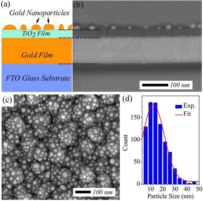
(Au-NPs/TiO2). RESULTS AND DISCUSSION As schematically shown in Fig. 1a, the near-perfect visible absorber employed in this study is a three-layered plasmonic nanostructure supported by a
fluorine-doped tin oxide (FTO) glass substrate. The bottommost layer of the structure is an optically thick Au film with a thickness of ~150 nm and the middle layer is a thin TiO2
semiconductor film. At the very top, there is a monolayer of Au NPs formed by thermal annealing of a very thin Au film pre-deposited on the TiO2 layer, in which the surface coverage and size
dispersion of the NPs can be controlled by the initial Au film thickness and the thermal annealing condition41. Previous studies have already demonstrated that the gap layer thickness and
the surface coverage and size dispersion of metal NPs could affect the overall absorption of the metal-dielectric-metal nanostructures36,37,38,39. Considering that the thermal annealing
process is also intentionally used here to transform the as-grown amorphous TiO2 film to polycrystalline anatase film structure (see Fig. S1 in Supporting Information), we perform the
thermal treatment in air atmosphere at 400 °C for 3 hours. Under this fixed annealing condition, the absorption is therefore determined by the thicknesses of the TiO2 gap layer and the
pre-deposited Au film. The optimum values of these two thicknesses leading to the strongest visible light absorption with the broadest possible bandwidth can be easily found through multiple
deposition experiments (see Methods). Figure 1b,c show respectively the side-view and top-view scanning electron microscope (SEM) images of the optimized Au-NPs/TiO2/Au-film nanostructure
prepared with a 5-nm-thick Au film pre-deposited on a 50-nm-thick TiO2 spacer layer. These SEM images reveal that the Au NPs with large size dispersion are distributed randomly on the TiO2
layer after the thermal annealing. Further analysis on the top-view SEM image (Fig. 1c) shows that the Au NPs occupy ~35% of the surface area and their sizes follow a Gaussian distribution
centered at 12 nm (Fig. 1d). To characterize the optical properties of the fabricated samples, the reflection and transmission are measured in an optical microscope coupled to a
visible/near-infrared spectrometer with absorption calculated as _A_ = 1–Transmission–Reflection (see Methods for detailed optical measurements). Figure 2a displays the absorption spectra of
the optimized Au-NPs/TiO2/Au-film nanostructure. For direct comparison, Fig. 2a also shows the absorption spectra of two control samples: a pure 50-nm-thick TiO2 film and a Au-NPs/TiO2
nanostructure. As expected, the pure TiO2 film only shows negligible absorption in the visible range (blue curve in Fig. 2a). For the Au-NPs/TiO2 nanostructure, optical absorption with a
maximum value of 40% (around the wavelength of 550 nm) and a full-width half-maximum (FWHM) of ~200 nm is observed (olive curve in Fig. 2a), which is due to the excitations of the
localized-SPRs supported by Au NPs20,21,23,24,25,26,27,28,29,30. As compared to the Au-NPs/TiO2 nanostructure, the optimized Au-NPs/TiO2/Au-film nanostructure appears quite dark in colour
(insets of Fig. 2a) and exhibits remarkably high ~90% average absorption in the entire visible spectrum 400–750 nm. Furthermore, the optical absorption of the optimized Au-NPs/TiO2/Au-film
nanostructure exhibits a negligible incident angle dependency (see Fig. S2 in Supporting Information), which is consistent with previously reported studies36,37,38,39. Figure 2b shows the
calculated normal incidence absorption spectrum of the Au-NPs/TiO2/Au-film nanostructure, which is conducted by using the three-dimensional finite-element-method (FEM) software COMSOL
Multiphysics. In the simulations, the Au-NPs/TiO2/Au-film nanostructure is approximated by a periodic super cell configuration consisting of a monolayer of circularly-shaped 20-nm-thick Au
disks with diameters randomly chosen from the analyzed Gaussian distribution (Fig. 1d) and a semi-infinite Au film separated by a 50-nm-thick TiO2 planar film. The subwavelength super cell
period of 100 nm is determined from the measured surface coverage of ~35% (inset of Fig. 2b). The dielectric constant of TiO2 is set to 3.9 and the permittivity of Au is taken from the
experimental data of Johnson and Christy42. It should be noted that the simulated absorption, especially within the wavelength range 600–700 nm, is slightly weaker than the measured
absorption, which may result from the approximations made in the simulations, such as smoothed TiO2 gap layer, Au NPs that are assumed to have circular shapes and uniform heights and the
imparted periodicity that is not present in the fabricated structure. Apart from this discrepancy, the calculated and measured results are in reasonable agreement with each other. Previous
studies have demonstrated that both the intrinsic losses and the plasmon-induced losses, which should respectively reside in the bottom metal layer and the top layer of metal NPs, could
contribute to the absorption obtained from the metal-dielectric-metal nanostructures37,43. However, these two loss mechanisms could play different roles in the generation of hot electrons,
as will be demonstrated later. Therefore, it is necessary to separately quantify contributions from these two different mechanisms in the Au-NPs/TiO2/Au-film nanostructure. To do this, the
absorption contributions from the top layer of Au NPs and the bottom Au film are calculated by integrating the power loss density over their respective volumes and shown in Fig. 2b. The
absorption contribution from the bottom Au film (orange curve in Fig. 2b) is found to coincide with the absorption spectrum calculated for an optically thick planar Au film (purple curve in
Fig. 2b), implying that the intrinsic losses are only affected weakly by the gap-plasmon resonances in the Au-NPs/TiO2/Au-film nanostructure. Furthermore, it is also seen that the intrinsic
loss is larger than the absorption contribution from the top layer of Au NPs within the wavelength range 400–517 nm. On the contrary, for the wavelengths longer than ~517 nm, the absorption
contribution from the top layer of Au NPs becomes exceedingly larger than the absorption contribution from the bottom Au film, revealing that the plasmon-induced absorption is the dominant
loss mechanism in this wavelength range. To evaluate the PEC performance of the prepared samples, the short-circuit photocurrent measurements are carried out in a three-electrode system
under zero external bias voltage (see Methods for detailed photocurrent measurements). Figure 3a shows the photocurrent versus time (_I_-_t_) curves for the Au-NPs/TiO2/Au-film nanostructure
(red curve), the pure TiO2 film (blue curve) and the Au-NPs/TiO2 nanostructure (olive curve) under illuminations of white light and visible light (λ > 420 nm and λ > 550 nm). The bare
TiO2 film produces a photocurrent density of ~1.5 μA/cm2 under light illumination of full spectrum (including UV region) and an ultra-small photocurrent density of ~0.02 μA/cm2 under
visible illumination (λ > 550 nm), which is consistent with the negligible visible light absorption of the TiO2 film (blue curve in Fig. 2a). However, due to the existence of possible
vacancy defects or chemical impurities30, our prepared TiO2 film is found to generate a relatively small photocurrent density of ~0.58 μA/cm2 under visible illumination (λ > 420 nm). When
the TiO2 film is decorated with Au NPs, corresponding to its enhanced visible light absorption, the observed photocurrent densities are increased to ~4.4 μA/cm2, ~3.7 μA/cm2 and ~2.6 μA/cm2
under light illuminations of full spectrum, λ > 420 nm and λ > 550 nm, respectively. Similar photocurrent enhancements have been observed in the previously reported metal-TiO2
nanostructures and have been attributed to the hot electrons generated from the non-radiative decay of the localized-SPRs in the Au-NPs20,21,23,24,25,26,27,28,29,30. With the goal of
expanding the energy utilization of TiO2 to the visible light based on the hot electron injection mechanism, it is necessary to increase the number of hot electrons generated upon light
absorption by the plasmonic nanostructures. As compared to the two control samples, the Au-NPs/TiO2/Au-film nanostructure possesses much stronger light absorption (Fig. 2a) and therefore, is
expected to correspondingly exhibit higher plasmonic-induced visible-light photoresponsivity. It is seen from Fig. 3a that the Au-NPs/TiO2/Au-film nanostructure indeed exhibits the highest
photocurrent density among all the three samples. Even under the visible (λ > 550 nm) illumination, the recorded photocurrent density in the Au-NPs/TiO2/Au-film nanostructure is as high
as ~15.8 μA/cm2, which is consistent with the value obtained from the linear sweep voltammagram (see Fig. S3 in Supporting Information) and is ~6 times the one obtained from the Au-NPs/TiO2
nanostructure under otherwise the same conditions. Figure 3b shows the experimental IPCE spectra of the Au-NPs/TiO2/Au-film nanostructure (red line) and the Au-NPs/TiO2 under zero external
bias voltage. At each center wavelength (λ, unit in nm) of a quasi-monochromatic light produced using a bandpass filter (10-nm-FWHM), the IPCE value is defined as IPCE = 1240_R_/λ, where _R_
= _I_/_J_ is the photoresponsivity, with _I_ being the measured photocurrent density (mA/cm2) and _J_ being the incident light power density (mW/cm2). The Au-NPs/TiO2/Au-film device shows
much higher IPCE values than the Au-NPs/TiO2, which coincides with the stronger broadband visible light absorption of the Au-NPs/TiO2/Au-film nanostructure. As shown in the inset of Fig. 3b,
the IPCE enhancement ratio of the Au-NPs/TiO2/Au-film nanostructure to the Au-NPs/TiO2 more clearly demonstrates that the enhancement is significant and reaches a particular high factor of
~5 over the entire wavelength range 450–850 nm. As already demonstrated above, both the intrinsic losses and the plasmon-induced losses contribute to the absorption of the
Au-NPs/TiO2/Au-film nanostructure (Fig. 2b). For the metal-dielectric-metal architecture shown in Fig. 1a, Schottky junctions can be formed at the interfaces between the TiO2 film and the
top layer of the Au NPs as well as the bottom Au film. These Schottky barriers allow hot electrons to be collected and injected from both the top and bottom Au-parts into the conduction band
of TiO2, producing photocurrents with opposite flow directions44, provided that hot electrons can be generated by the above mentioned different loss mechanisms. At short wavelengths (λ <
517 nm), because the intrinsic losses in the bottom Au film are larger than the plasmon-induced losses in the top layer of Au NPs (Fig. 2b), more hot electrons are expected to be
transmitted from the bottom contact to the top contact than in the opposite direction. By contrast, it is expected to see that hot electrons are mainly transmitted from the top to the bottom
contact at long wavelengths (λ > 517 nm), owing to the dominant plasmon-induced losses in the top layer of Au NPs (Fig. 2b). However, the detected photocurrents under illumination of
quasi-monochromatic light with wavelengths of 450 nm and 650 nm are found to have the same flow directions, running from the top to bottom contact (see Fig. S4 in Supporting Information).
This implies that the intrinsic losses have almost no contribution to the generation of hot electrons (and thus the photocurrent). As a result, only the plasmon-induced losses in the top
layer of Au NPs need to be considered in the hot electron generation and transfer process. According to the modified Fowler relation22, the quantum efficiency of hot electrons across the
Schottky barrier can be approximated as η = _C__F_(_hν_ − _qϕ__b_)2/_hν_, with _C__F_ being the Fowler emission coefficient, _hυ_ being the photon energy and _qϕ__b_ being the barrier
height. Figure 3c (blue line) shows the calculated quantum efficiency spectrum of the Au-TiO2 junction with a barrier height of _qϕ__b_ ≈ 0.96 eV 19, which reveals much higher value in the
shorter wavelengths and decreases gradually as increasing the incident wavelengths. With the already obtained spectrum of the absorption contribution from the top layer of Au NPs (_A_) and
the above-calculated quantum efficiency spectrum (η), the photoresponsivity spectrum _R_ can be given by _R_ = _Aη_ 22 and consequently the IPCE spectrum can be calculated as IPCE = 1240
_R_/λ. The line shape of the calculated IPCE spectrum of the Au-NPs/TiO2/Au-film nanostructure (red solid line in Fig. 3c) is very similar to the experimentally measured one (red line in
Fig. 3b), clearly demonstrating that the gap-plasmon supported by the Au-NPs/TiO2/Au-film nanostructure plays a key role in the PEC performance improvement. The PEC water splitting
performances of the prepared Au-NPs/TiO2/Au-film and Au-NPs/TiO2 nanostructures are also directly examined (see Methods for detailed hydrogen and oxygen measurements). Figure 4 shows both
the hydrogen and oxygen evolution under illumination of visible light (λ > 550 nm) as a function of illumination duration. For the Au-NPs/TiO2 nanostructure, hydrogen production could not
be detected after 1 h-illumination. When the illumination duration is increased to 2 h–5 h, the hydrogen generation density evolved from the Au-NPs/TiO2 nanostructure is found to be about
0.12, 0.16, 0.24 and 0.30 μmol/cm2, respectively (blue patterns in Fig. 4). By linearly fitting the dependence of the hydrogen generation density on the illumination duration, the hydrogen
generation rate is found to be ~0.06 μmol/h∙cm2. It should be noted that even after 5 h visible light illumination the amount of the oxygen evolved from the Au-NPs/TiO2 nanostructure is
still below the detection limit. For the Au-NPs/TiO2/Au-film device, the hydrogen generation density of ~0.22 μmol/cm2 is readily to be detected after 1 h illumination and is found to be
almost linearly increased from ~0.38 μmol/cm2 to ~1.08 μmol/cm2 with increasing the illumination duration from 2 h to 5 h (blue pattern in Fig. 4). The hydrogen generation rate obtained from
linear fitting is ~0.21 μmol/h∙cm2 for the Au-NPs/TiO2/Au-film device, which is over 3 times the one obtained from the Au-NPs/TiO2 nanostructure. Furthermore, the oxygen generation density
of ~0.28 μmol/cm2 is detected from the Au-NPs/TiO2/Au-film nanostructure after 3 h visible light illumination and is increased from ~0.43 μmol/cm2 to ~0.54 μmol/cm2 with increasing the
illumination duration from 4 h to 5 h (olive pattern in Fig. 4). The oxygen generation rate obtained from linear fitting is ~0.11 μmol/h∙cm2, which is almost half of the obtained hydrogen
generation rate (~0.21 μmol/h∙cm2) and thus confirming that the hydrogen and oxygen are evolved at the expected stoichiometric ratio in PEC water-splitting experiment. The above results
clearly demonstrate that the Au-NPs/TiO2/Au-film nanostructure exhibits much improved PEC performance, which in turn confirms that increasing the absorption of incident photons in the
plasmonic catalysts can enhance the generation of hot electrons and photocurrents. It is also worth noting that no noticeable degradation in the PEC performance of the Au-NPs/TiO2/Au-film
device is observed after 5 sequential 1 h–5 h runs (total 15 h-illumination), which is consistent with previously reported study24,29 and indicates that the operational lifetime of Au-TiO2
based plasmonic photocatalysts could exceed that of the efficient water splitters based on semiconductors29. In summary, we experimentally demonstrate that the Au-NPs/TiO2/Au-film
nanostructure is capable of providing a broadband near-perfect visible light absorption. Such greatly enhanced broadband light absorption in the Au-NPs/TiO2/Au-film nanostructure could
overcome the shortcomings such as the narrowband and insufficient resonant light absorption in the conventional plasmonic-TiO2 photocatalysts20,21,23,24,25,26,27,28,29,30 and thus could be
exploited to enhance the generation of hot electrons and photocurrents. We show that a 5-fold-enhanced incident photon-to-current conversion efficiency is achieved within the entire
wavelength range 450–850 nm in the Au-NPs/TiO2/Au-film device, as compared to the Au-NPs/TiO2 nanostructures. Although the achieved efficiency of the plasmonic device is still lower than
that of the conventional solar cells due to the loss of hot electrons via ultrafast electron-electron scattering21, our present work can give an impetus to the fabrication of simple
nanostructures for hot-electron based plasmonic catalysts. For practical applications, the PEC performance of the plasmonic device needs to be improved, which may be accomplished by
introducing some other enhancement mechanisms, such as oxygen evolution catalyst26, roughening the metal/semiconductor interface45 and using graphene as hot electron receiver46. In
particular, plasmon induced interfacial charge transfer transition has been recently reported as a new hot-electron transfer mechanism with a quantum yield for electron injection of 24%47.
We hope that combing this fast hot-electron injection mechanism into the metal-dielectric-metal based plasmonic photocatalysts with near-perfect broadband absorption will allow the
efficiency of the plasmonic device in excess of 24%. METHODS Au and TiO2 films were deposited by radio frequency (RF) magnetron sputtering. Cleaned FTO glasses (1.5 × 2 cm2) were used as
supporting substrates and placed parallel to the target at a distance of 60 mm. The chamber pressure was first pumped down to 1 × 10⁻⁴ Pa, then argon was introduced to a pressure of 1.5 Pa.
The TiO2 and Au targets were powered by an RF generator at a frequency of 13.56 MHz and were pre-sputtering in argon for 3 minutes before each deposition step. The control sample of the pure
TiO2 film was prepared by depositing TiO2directly onto the FTO substrate. The control sample of the Au-nanoparticles loaded TiO2 film was prepared by successively depositing TiO2 and Au
onto the FTO substrate. For preparing the Au-NPs/TiO2/Au-film nanostructures, an optically thick (150 nm) Au layer was first deposited onto the FTO substrate. After that, TiO2 and Au were
successively sputtered onto the as-deposited Au layer. The thicknesses of the TiO2 layer and the top layer Au film were varied to find the optimum values to make the Au-NPs/TiO2/Au-film
nanostructure achieve the strongest visible light absorption with the broadest possible bandwidth. All the as-prepared samples were annealed in air atmosphere at 400 °C for 3 hours to form
the Au nanoparticles and simultaneously transform the amorphous TiO2 film to polycrystalline anatase film structure. The reflection and transmission spectra measurements were performed with
an optical microscope. The samples were illuminated by un-polarized white light from a halogen lamp focused by a microscope objective. The reflected light from the samples was collected by
the same objective lens, while the transmitted light was collected by a microscope condenser. The collected light was then analyzed by a visible/near-infrared spectrometer. The measured
transmission spectra (_T_) were normalized with a transmission spectrum of a cleaned FTO glass substrate and the reflection spectra (_R_) were normalized with a reflection spectrum collected
on a silver mirror. For the bare TiO2 film and the Au-nanoparticles loaded TiO2 film (two control samples), the experimental absorption spectra were derived by _A_ = 1 − _T_ − _R_. The
bottom Au film in the Au-NPs/TiO2/Au-film nanostructure is thick enough to eliminate the optical light transmission (_T_ = 0). Therefore, only the reflection spectra needed to be measured
for the Au-NPs/TiO2/Au-film nanostructures and the absorption spectra were given by _A_ = 1 − _R_. To measure the photocurrent, all the prepared samples were connected to the electrochemical
workstation (CHI 660E) as the working electrode. A platinum wire and a saturated calomel electrode (SCE) were used as the counter and reference electrodes, respectively. An aqueous KOH
(1Mol l−1, PH = 14) was used as the electrolyte solution. The area of the sample exposed to light was ~0.25 cm2. The photocurrent measurements under illumination of white light were carried
out directly with a 300 W xenon lamp source. Long-pass filters with a cut-on wavelength of 420 nm and 550 nm were placed in the light path to simulate the visible illuminations of λ > 420
nm and λ > 550 nm, respectively. Action spectrum was obtained by a semi-monochromatic irradiation produced through a series of band pass filters with different center wavelengths (10 nm
full widths at half-maximum). The wavelength dependent light intensity was measured by a spectroradiometer (Newport 1918-C). To quantitatively determine the amount of evolved H2 and O2
resulting from the reduction of water, the three-electrode system same as that used in the photocurrent measurement was employed, in which an aqueous KOH solution (1Mol l−1, PH = 14) was
also used as the electrolyte solution and the area of the sample exposed to light was ~2 cm2. The gas collected from the platinum counter electrode was analyzed by gas chromatography-mass
spectroscopy (GC-MS). ADDITIONAL INFORMATION HOW TO CITE THIS ARTICLE: Lu, Y. _et al._ Gap-plasmon based broadband absorbers for enhanced hot-electron and photocurrent generation. _Sci.
Rep._ 6, 30650; doi: 10.1038/srep30650 (2016). REFERENCES * Tachibana, Y., Vayssieres, L. & Durrant, J. R. Artificial Photosynthesis for Solar Water-Splitting. Nat. Photonics 6, 511–518
(2012). Article ADS CAS Google Scholar * Fujishima, A. & Honda, K. Electrochemical Photolysis of Water at a Semiconductor Electrode. Nature 238, 37–38 (1972). ADS CAS PubMed
Google Scholar * Wang, G. et al. Hydrogen-Treated TiO2 Nanowire Arrays for Photoelectrochemical Water Splitting. Nano Lett. 11, 3026–3033 (2011). Article ADS CAS PubMed Google Scholar
* Cho, I. S. et al. Branched TiO2 Nanorods for Photoelectrochemical Hydrogen Production. Nano Lett. 11, 4978–4984 (2011). Article ADS CAS PubMed Google Scholar * Mohapatra, S. K.,
Misra, M., Mahajan, V. K. & Raja, K. S. Design of a Highly Efficient Photoelectrolytic Cell for Hydrogen Generation by Water Splitting: Application of TiO2-xCx Nanotubes as a Photoanode
and Pt/TiO2 Nanotubes as a Cathode. J. Phys. Chem. C 111, 8677–8685 (2007). Article CAS Google Scholar * Noh, S. Y. et al. Branched TiO2/Si Nanostructures for Enhanced
Photoelectrochemical Water Splitting. Nano Energy. 2, 351–360 (2013). Article CAS Google Scholar * Lin, Y. et al. Semiconductor Nanostructure-Based Photoelectrochemical Water Splitting: A
Brief Review. Chem. Phys. Lett. 507, 209–215 (2011). Article ADS CAS Google Scholar * Asahi, R., Morikawa, T., Ohwaki, T., Aoki, K. & Taga, Y. Visible-Light Photocatalysis in
Nitrogen-Doped Titanium Oxides. Science 293, 269–271 (2001). Article CAS PubMed Google Scholar * Park, J. H., Kim, S. & Bard, A. J. Novel Carbon-Doped TiO2 Nanotube Arrays with High
Aspect Ratios for Efficient Solar Water Splitting. Nano Lett. 6, 24–28 (2006). Article ADS CAS PubMed Google Scholar * Xu, M., Da, P., Wu, H., Zhao, D. & Zheng, G. Controlled
Sn-Doping in TiO2 Nanowire Photoanodes with Enhanced Photoelectrochemical Conversion. Nano Lett. 12, 1503–1508 (2012). Article ADS CAS PubMed Google Scholar * Wang, G. et al.
Hydrogen-Treated TiO2 Nanowire Arrays for Photoelectrochemical Water Splitting. Nano Lett. 11, 3026–3033 (2011). Article ADS CAS PubMed Google Scholar * Petrik, N. G. et al. Chemical
Reactivity of Reduced TiO2(110): The Dominant Role of Surface Defects in Oxygen Chemisorption. J. Phys. Chem. C 113, 12407–12411 (2009). Article CAS Google Scholar * Brown, M. D. et al.
Plasmonic Dye-Sensitized Solar Cells Using Core−Shell Metal−Insulator Nanoparticles. Nano Lett. 11, 438–445 (2011). Article ADS CAS PubMed Google Scholar * O’Regan, B. & Grätzel, M.
A Low-Cost, High-Efficiency Solar Cell Based on Dye-Sensitized Colloidal TiO2 Films. Nature 353, 737–740 (1991). Article ADS Google Scholar * Chen, H. et al. Computational Modeling of
Plasmon-Enhanced Light Absorption in a Multicomponent Dye Sensitized Solar Cell. J. Phys. Chem. C 116, 10215–10221 (2012). Article ADS CAS Google Scholar * Wang, C. L. et al.
Sonoelectrochemical Synthesis of Highly Photoelectrochemically Active TiO2 Nanotubes by Incorporating CdS Nanoparticles. Nanotechnology 20, 295601–295606 (2009). Article PubMed CAS Google
Scholar * Wu, Q. et al. Ultrasound-Assisted Synthesis and Visible-Light-Driven Photocatalytic Activity of Fe-Incorporated TiO2 nNanotube Array Photocatalysts. J. Hazard. Mater. 199–200,
410–417 (2012). Article ADS PubMed CAS Google Scholar * Wang, M. Y. et al. p–n Heterojunction Photoelectrodes Composed of Cu2O-Loaded TiO2 Nanotube Arrays with Enhanced
Photoelectrochemical and Photoelectrocatalytic Activities _Energy_ Environ. Sci. 6, 1211–1220 (2013). CAS Google Scholar * Zhang, X. M., Chen, Y. L., Liu, R. S. & Tsai, D. P. The
Self-Assembly, Aggregation and Phase Transitions of Food Protein Systems in One, Two and Three Dimensions. Rep. Prog. Phys. 76, 046401–046443 (2013). ADS PubMed Google Scholar * Linic,
S., Christopher, P. & Ingram, D. B. Plasmonic-Metal Nanostructures for Efficient Conversion of Solar to Chemical Energy. Nat. Mater. 10, 911–921 (2011). Article ADS CAS PubMed Google
Scholar * Clavero, C. Plasmon-Induced Hot-Electron Generation at Nanoparticle/Metal-Oxide Interfaces for Photovoltaic and Photocatalytic Devices. Nat. Photonics 8, 95–103 (2014). Article
ADS CAS Google Scholar * Knight, M. W., Sobhani, H., Nordlander, P. & Halas, N. J. Photodetection with Active Optical Antennas. Science 332, 702–704 (2011). Article ADS CAS PubMed
Google Scholar * Tian, Y. & Tatsuma, T. Mechanisms and Applications of Plasmon-Induced Charge Separation at TiO2 Films Loaded with Gold Nanoparticles. J. Am. Chem. Soc. 127, 7632–7637
(2005). Article CAS PubMed Google Scholar * Nishijima, Y., Ueno, K., Yokota, Y., Murakoshi, K. & Misawa, H. Plasmon-Assisted Photocurrent Generation from Visible to Near-Infrared
Wavelength Using a Au-Nanorods/TiO2 Electrode. J. Phys. Chem. Lett. 1, 2031–2036 (2010). Article CAS Google Scholar * Mubeen, S., Hernandez-Sosa, G., Moses, D., Lee, J. & Moskovits,
M. Plasmonic Photosensitization of a Wide Band Gap Semiconductor: Converting Plasmons to Charge Carriers. Nano Lett. 11, 5548–5552 (2011). Article ADS CAS PubMed Google Scholar * Lee,
J., Mubeen, S., Ji, X. L., Stucky, G. D. & Moskovits, M. Plasmonic Photoanodes for Solar Water Splitting with Visible Light. Nano Lett. 12, 5014–5019 (2012). Article ADS CAS PubMed
Google Scholar * Zhang, Z. H., Zhang, L. B., Hedhili, M. N., Zhang, H. N. & Wang, P. Plasmonic Gold Nanocrystals Coupled with Photonic Crystal Seamlessly on TiO2 Nanotube
Photoelectrodes for Efficient Visible Light Photoelectrochemical Water Splitting. Nano Lett. 13, 14–20 (2013). Article ADS CAS PubMed Google Scholar * Shi, X., Ueno, K., Takabayashi, N.
& Misawa, H. Plasmon-Enhanced Photocurrent Generation and Water Oxidation with a Gold Nanoisland-Loaded Titanium Dioxide Photoelectrode. J. Phys. Chem. C 117, 2494–2499 (2013). Article
CAS Google Scholar * Mubeen, S. et al. An Autonomous Photosynthetic Device in Which All Charge Carriers Derive from Surface Plasmons. Nat. Nanotechnology 8, 247–251 (2013). Article ADS
CAS Google Scholar * Chen, W. J., Lu, Y. H., Dong, W., Chen, Z. & Shen, M. R. Plasmon mediated Visible Light Photocurrent and Photoelectrochemical Hydrogen Generation Using Au
Nanoparticles/TiO2 Electrode. Mater. Res. Bull. 50, 31–35 (2014). Article CAS Google Scholar * Lin, K. T., Chen, H. L., Lai, Y. S. & Yu, C. C. Silicon-Based Broadband Antenna for High
Responsivity and Polarization-Insensitive Photodetection at Telecommunication Wavelengths. Nat. Communications 5, 3288–3288 (2014). Article ADS CAS Google Scholar * Li, W. &
Valentine, J. Metamaterial Perfect Absorber Based Hot Electron Photodetection. Nano Lett. 14, 3510–3514 (2014). Article ADS CAS PubMed Google Scholar * Aydin, K., Ferry, V. E., Briggs,
R. M. & Atwater, H. A. Broadband Polarization-Independent Resonant Light Absorption Using Ultrathin Plasmonic Super Absorbers. Nat. Communications 2, 193–198 (2011). Article CAS Google
Scholar * Hao, J. et al. High Performance Optical Absorber Based on A Plasmonic Metamaterial. Appl. Phys. Lett. 96, 251104–3 (2010). Article ADS CAS Google Scholar * Liu, N., Mesch,
M., Weiss, T., Hentschel, M. & Giessen, H. Infrared Perfect Absorber and Its Application as Plasmonic Sensor. Nano Lett. 10, 2342–2348 (2010). Article ADS CAS PubMed Google Scholar
* Moreau, A. et al. Controlled-Reflectance Surfaces with Film-Coupled Colloidal Nanoantennas. Nature 492, 86–89 (2012). Article ADS CAS PubMed PubMed Central Google Scholar * Nielsen,
M. G., Pors, A., Albrektsen, O. & Bozhevolnyi, S. I. Efficient Absorption of Visible Radiation by Gap Plasmon Resonators. Opt. Express 20, 13311–13319 (2012). Article ADS PubMed
Google Scholar * Hedayati, M. K. et al. Design of A Perfect Black Absorber at Visible Frequencies Using Plasmonic Metamaterials. Adv. Mater. 23, 5410–5414 (2011). Article CAS PubMed
Google Scholar * Wang, D., Zhu, W., Best, M. D., Camden, J. P. & Crozier, K. B. Wafer-Scale Metasurface for Total Power Absorption, Local Field Enhancement and Single Molecule Raman
Spectroscopy. Sci. Rep. 3, 2867–6 (2013). Article ADS PubMed PubMed Central Google Scholar * Zhang, Y. et al. Vapor-Deposited Amorphous Metamaterials as Visible Near-Perfect Absorbers
with Random Non-Prefabricated Metal Nanoparticles. Sci. Rep. 4, 4850–4855 (2014). Article CAS PubMed PubMed Central Google Scholar * Presland, A. E. B., Price, G. L. & Trimm, D. L.
Hillock Formation by Surface Diffusion on Thin Silver Films. Surf. Sci. 29, 424–434 (1972). Article ADS CAS Google Scholar * Johnson, P. B. & Christy, R. W. Optical Constants of the
Noble Metals. Phys. Rev. B 6, 4370–4379 (1972). Article ADS CAS Google Scholar * Li, W. et al. Refractory Plasmonics with Titanium Nitride: Broadband Metamaterial Absorber. Adv. Mater.
26, 7959–7965 (2014). Article ADS CAS PubMed Google Scholar * Chalabi, H., Schoen, D. & Brongersma, M. L. Hot-Electron Photodetection with a Plasmonic Nanostripe Antenna. Nano Lett.
14, 1374–1380 (2014). Article ADS CAS PubMed Google Scholar * Goykhman, I., Desiatov, B., Khurgin, J., Shappir, J. & Levy, U. Waveguide based compact silicon Schottky photodetector
with enhanced responsivity in the telecom spectral band. Opt. Express 20, 28954–28602 (2012). Article Google Scholar * Fang, Z. et al. Graphene-Antenna Sandwich Photodetector. Nano Lett.
12, 3808–3813 (2012). Article ADS CAS PubMed Google Scholar * Wu, K., Chen, J., Mcbride, J. R. & Lian, T. Efficient hot-electron transfer by a plasmon-induced interfacial
charge-transfer transition. Science 349, 632–635 (2015). Article ADS CAS PubMed Google Scholar Download references ACKNOWLEDGEMENTS We acknowledge financial support from the State Key
Program for Basic Research of China (SKPBRC) under Grant Nos 2012CB921501 and 2013CB632703, the National Nature Science Foundation of China (NSFC) under Grant Nos 11174137 and 11474215 and
the Priority Academic Program Development of Jiangsu Higher Education Institutions (PAPD). AP and SIB acknowledge financial support from the University of Southern Denmark (SDU 2020 funding)
and the Danish Council for Independent Research (the FTP project PlasTPV, contract no. 1335-00104). AUTHOR INFORMATION AUTHORS AND AFFILIATIONS * College of Physics, Optoelectronics and
Energy, Collaborative Innovation Center of Suzhou Nano Science and Jiangsu Key Laboratory of Thin Films, Soochow University, Suzhou, 215006, China Yuhua Lu & Wen Dong * School of Physics
and National Laboratory of Solid State Microstructures, Nanjing University, Nanjing, 210093, China Zhuo Chen & Zhenlin Wang * Centre for Nano Optics, University of Southern Denmark,
Campusvej 55, Odense M, DK-5230, Denmark Anders Pors & Sergey I. Bozhevolnyi Authors * Yuhua Lu View author publications You can also search for this author inPubMed Google Scholar * Wen
Dong View author publications You can also search for this author inPubMed Google Scholar * Zhuo Chen View author publications You can also search for this author inPubMed Google Scholar *
Anders Pors View author publications You can also search for this author inPubMed Google Scholar * Zhenlin Wang View author publications You can also search for this author inPubMed Google
Scholar * Sergey I. Bozhevolnyi View author publications You can also search for this author inPubMed Google Scholar CONTRIBUTIONS W.D. and Z.C. conceived the idea. Y.L. and W.D. fabricated
the devices. A.P. and Z.C. performed calculations. S.I.B., Z.W. and Z.C. analyzed the data and wrote the manuscript. All authors carefully revised the manuscript before the submission.
ETHICS DECLARATIONS COMPETING INTERESTS The authors declare no competing financial interests. ELECTRONIC SUPPLEMENTARY MATERIAL SUPPLEMENTARY INFORMATION RIGHTS AND PERMISSIONS This work is
licensed under a Creative Commons Attribution 4.0 International License. The images or other third party material in this article are included in the article’s Creative Commons license,
unless indicated otherwise in the credit line; if the material is not included under the Creative Commons license, users will need to obtain permission from the license holder to reproduce
the material. To view a copy of this license, visit http://creativecommons.org/licenses/by/4.0/ Reprints and permissions ABOUT THIS ARTICLE CITE THIS ARTICLE Lu, Y., Dong, W., Chen, Z. _et
al._ Gap-plasmon based broadband absorbers for enhanced hot-electron and photocurrent generation. _Sci Rep_ 6, 30650 (2016). https://doi.org/10.1038/srep30650 Download citation * Received:
03 March 2016 * Accepted: 08 July 2016 * Published: 29 July 2016 * DOI: https://doi.org/10.1038/srep30650 SHARE THIS ARTICLE Anyone you share the following link with will be able to read
this content: Get shareable link Sorry, a shareable link is not currently available for this article. Copy to clipboard Provided by the Springer Nature SharedIt content-sharing initiative