Functionalized thallium antimony films as excellent candidates for large-gap quantum spin hall insulator
- Select a language for the TTS:
- UK English Female
- UK English Male
- US English Female
- US English Male
- Australian Female
- Australian Male
- Language selected: (auto detect) - EN
Play all audios:
ABSTRACT Group III-V films are of great importance for their potential application in spintronics and quantum computing. Search for two-dimensional III-V films with a nontrivial large-gap
are quite crucial for the realization of dissipationless transport edge channels using quantum spin Hall (QSH) effects. Here we use first-principles calculations to predict a class of
large-gap QSH insulators in functionalized TlSb monolayers (TlSbX2; (X = H, F, Cl, Br, I)), with sizable bulk gaps as large as 0.22 ~ 0.40 eV. The QSH state is identified by Z2 topological
invariant together with helical edge states induced by spin-orbit coupling (SOC). Noticeably, the inverted band gap in the nontrivial states can be effectively tuned by the electric field
and strain. Additionally, these films on BN substrate also maintain a nontrivial QSH state, which harbors a Dirac cone lying within the band gap. These findings may shed new light in future
design and fabrication of QSH insulators based on two-dimensional honeycomb lattices in spintronics. SIMILAR CONTENT BEING VIEWED BY OTHERS LARGE-BAND-GAP NON-DIRAC QUANTUM SPIN HALL STATES
AND STRONG RASHBA EFFECT IN FUNCTIONALIZED THALLENE FILMS Article Open access 25 September 2023 ANTIFERROMAGNETISM-DRIVEN TWO-DIMENSIONAL TOPOLOGICAL NODAL-POINT SUPERCONDUCTIVITY Article
Open access 04 February 2023 ANOMALOUS LANDAU QUANTIZATION IN INTRINSIC MAGNETIC TOPOLOGICAL INSULATORS Article Open access 09 August 2023 INTRODUCTION One of the grand challenges in
condensed matter physics and material science is to develop room-temperature electron conduction without dissipation. Two-dimensional (2D) topological insulators (TIs), namely quantum spin
Hall (QSH) insulators, are new states of quantum matter with an insulating bulk and metallic edge states1,2,3,4,5. Their helical edge states are spin-locked due to the protection of
time-reversal symmetry (TRS), namely the propagation direction of surface electrons is robustly linked to their spin orientation6, leading to dissipationless transport edge channels.
However, the working temperature of QSH insulators in experiments like HgTe/CdTe7,8 and InAs/GaSb films9,10 are very low (below 10 K), limited by their small energy gap. The search of QSH
insulators with large-gap is urgently required. Chemical functionalization of 2D materials is an effective way to realize QSH state with desirable large-gaps. The most reported cases include
hydrogenated or halogenated stanene11,12,13 and plumbene14 films. These films are QSH insulators with gaps as large as 0.2 ~ 1.34 eV, sufficient for practical applications at room
temperature. Group V films, including As15, Bi16 and Sb17, are large-gap QSH insulators, when functionalized with hydrogen or halogens. Recently, the organic molecule ethynyl-functionalized
stanene18,19 films have been reported to be good QSH insulators in the previous works. Progress also undergoes simultaneously in experiments, Bi (111) film has been successfully grown on
Bi2Te3 or Bi2Se3 substrates20,21,22,23. The common feature of these materials is that they all own 2D honeycomb-like crystal structures, indicating that 2D hexagonal lattice could be an
excellent cradle to breed QSH insulators with SOC. These large-gap QSH insulators are essential for realizing many exotic phenomena and for fabricating new quantum devices that can operate
at room temperature. Group III-V materials are of importance applicable to semiconductor devices in semiconductor industry. Especially, the π bonding between _p_z orbitals on group-III and V
atoms can generally open a bulk gap with SOC, similar to graphene1. Different from the inversion-symmetry (IS) in graphene, the geometry of group III-V films is not IS (inversion-asymmetry)
due to IS breaking. The previous works have shown that the not IS materials host many nontrivial phenomena such as the crystalline- surface-dependent topological electronic states24,25,
pyroelectricity26, topological _p-n_ junctions27, as well as topological superconductivity28,29, _et al_. However, one important characteristic of III-V films is that its unsaturated _p_z
orbital is chemically active, due to the weak π-π interaction as caused by the bond length between III-V atoms (~3 Å). This feature, together with the out-of-plane orientation of _p_z
orbital, facilitates strong orbital interaction with external environments and thus its electronic properties are easily affected by adsorbates and substrates, unfavorable for practical
applications in spintroncis. As a representative, here we provide a systematical study on structural and topological properties of 2D TlSb monolayers functionalized with hydrogen and
halogens, namely TlSbX2 (X = H, F, Cl, Br, I). We find that the surface functionalization on TlSb, _i.e._, saturating the _p_z orbital composed of TISb with hydrogen or halogens, can
stabilize the 2D TlSb, according to the calculated phonon spectrum of TlSbX2 films. All the systems are found to be QSH insulators, with the bulk gap in the range of 0.22 ~ 0.40 eV, tunable
by external strain and electric field. A single pair of topologically protected helical edge states is established for these systems with the Dirac point locating in the bulk gap and the odd
numbers of crossings between edge states and Fermi level prove the nontrivial nature of these TlSbX2 films. These findings may provide a new platform to design large-gap QSH insulator based
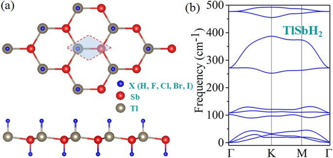
on group III-V films, which is important for device application in spintronics. RESULTS AND DISCUSSION The geometric structure of TlSbX2 (X = H, F, Cl, Br, I) are displayed in Fig. 1(a), in
which the Tl or Sb atoms are saturated with X atoms on both sides of the plane in an alternating manner along the hexagonal axis and thus breaks IS of TlSbX2. Table 1 lists the calculated
equilibrium lattice constants, buckling heights, as well as Tl-Sb, Tl-X and Sb-X bond lengths after structural optimization. In comparison to pristine TlSb, the TI-Sb bonds in TlSbX2
slightly expand, while the buckling changes differently due to the weakly hybridization between π and σ orbitals, stabilizing these structures. The stability of functionalized TlSbX2 is
studied through the formation energy defined as where _E_TlSbX2, _E_TISb and _E_X are the total energy of double-side functionalized TlSbX2, pristine TlSb and molecule X2, respectively. _N_X
is the number of X atoms. The calculated formation energies for TlSbH2, TlSbF2, TlSbCl2, TlSbBr2 and TlSbI2, are −1.862, −2.997, −1.613, −1.567 and −1.420 eV, respectively, suggesting that
hydrogen or halogens are chemically bonded to TlSb, indicating a higher thermodynamic stability relative to their elemental reservoirs. The dynamic stability of TlSbH2, as an example, is
further confirmed by the phonon dispersion curves in Fig. 1(b), in which all branches have positive frequencies and no imaginary phonon modes, confirming the stability of TlSbH2. Figure
2(a,d) display the calculated band structure for TlSbH2 and TlSbF2 as representative examples, in which the red and blue lines correspond to band structures without and with SOC. In the
absence of SOC, they are both gapless semimetal with the valence band maximum (VBM) and conduction band minimum (CBM) degenerate at the Fermi level. When takes SOC into account, the band
structures of TlSbH2 and TlSbF2 produce a semimetal-to-semiconductor transition, with sizeable bulk-gaps of 0.22 eV and 0.40 eV, respectively. As observed in previously reported 2D TIs like
ZeTe530, HfTe531 and GaSe32, graphene-like materials33,34,35, the SOC-induced band-gap opening at the Fermi level is a strong indication of the existence of topologically nontrivial phases.
An important character of the QSH insulator is helical edge states which is key to spintronic applications due to the ability to conduct dissipationless currents. Thus, we calculate the
topological edge states by the Wannier90 package36. We construct the maximally localized Wannier functions (MLWFs) and fit a tight-binding Hamiltonian with these functions. The calculated
edge Green’s function37 of semi-infinite TlSbX2 (X = H, F) is shown in Fig. 3(a,d). One can see that all the edge bands connect completely the conduction and valence bands and span 2D bulk
band gap, yielding a 1D gapless edge states. Besides, the counter-propagating edge states exhibit opposite spin-polarization, in accordance with the spin-momentum locking of 1D helical
electrons. In addition, the Dirac point located at the band gap are calculated to have a high velocity of ~2.0 × 10⁵ m/s, comparable to that of 5.5 × 10⁵ m/s in HgTe/CdTe quantum well7,8.
All these consistently indicate that TlSbX2 (X = H, F) are ideal 2D TIs. The topological states can be further confirmed by calculating topological invariant Z2 after the band inversion. Due
to IS breaking in TlSbX2, the method proposed by Fu and Kane38 cannot be used to calculate the Z2 invariant. Thus, a method independent of the presence of IS is needed. As reported by Yu
_et al_.39, we employ a recently proposed equivalent method for the Z2 topological invariant based on the U(2N) non-Abelian Berry connection. This approach allows the identification of the
topological nature of a general band insulator without any of the gauge-fixing problems that plague the concrete, previous implementation of invariants. Here, we introduce the evolution of
Wannier Center of Charges (WCCs)39 to calculate the Z2 invariant, which can be expressed as: which indicates the change of time-reversal polarization () between the 0 and _T_/2. The
evolution of the WCC along _ky_ corresponds to the phase factor, θ, of the eigenvalues of the position operator,, projected into the occupied subspace. Then the WFs related with lattice
vector _R_ can be written as: Here, a WCC can be defined as the mean value of , where theis the position operator and is the state corresponding to a WF in the cell with _R_ = 0. Then we can
obtain Assuming that with _S_ = _I_ or _II_, where summation in α represents the occupied states and _A_ is the Berry connection. So we have the format of Z2 invariant: The Z2 invariant can
be obtained by counting the even or odd number of crossings of any arbitrary horizontal reference line. In Fig. 3(c,f), we display the evolution lines of Wannier function centers (WFC) for
TlSbH2 and TlSbF2, respectively. It can be seen that the WFC evolution curves cross any arbitrary reference lines odd times, thus yielding Z2 = 1. Now, we turn to the physics of QSH effect
in TlSbX2. Since the decorated atoms hybridizes strongly with the dangling bonds of _p__z_ orbital in TISb, it effectively removes the _p__z_ bands away from the Fermi level, leaving only
the _s_ and _p_x,y orbitals, as displayed in Fig. 2(b,c,e,f). However, through projecting the bands onto different atomic orbitals, we find that there are two scenarios for the effect of SOC
on the bands around the Fermi level, in which the _s_ and _p__x,y_ band inversion are different from each other. For TlSbH2, at the Γ point, the two _p__x,y_ orbitals from TI and Sb atoms
are energy degenerate, while the bands away from the Γ point are well separated due to orbital splitting. The Fermi level is located between one _s_ and two _p__x,y_ orbitals, rendering the
_s_ above _p__x,y_ orbitals in energy, thus forming a normal band order, similar to the cases in conventional III-V semiconductors. While for TlSbF2, the band structures are changed
drastically, as shown in Fig. 2(d–f). In sharp contrast to TlSbH2, the band order at the Γ point is inverted, _i.e._, the _s_ is shifted below two _p__x,y_ orbitals. These two different band
orders may be attributed to the chemical bonding and orbital splitting between TI and Sb atoms. To further understand the physics of band inversion, we display in Fig. 4 the schematic of
orbital inversion at the Γ point around the Fermi level in TlSbH2 and TlSbF2 films. On can see that, the chemical bonding and crystal field splitting between TI and Sb atoms make the _s_ and
_p_x,y orbital split into the bonding and anti-bonding states, _i.e., s_± and _p_±x,y, which the superscripts + and − represent the parities of corresponding states, respectively. As
displayed in Fig. 4(a), the _s_+ orbital for hydrogenated one is significantly higher somewhere above _p_−x,y orbital of Tl and Sb atoms under the effect of crystal field. The inclusion of
SOC makes the degeneracy of _p_−x,y orbital split into _p_−x + iy,↑& _p_−x−iy,↓ and _p_−x−iy,↑& _p_−x + iy,↓, leading _s_+ locate in between them. On the other hand, for TlSbF2 in
Fig. 4(b), the larger lattice constant results in a weaker _s_-_p_ hybridization and accordingly a smaller energy separation between the bonding and anti-bonding states. Thus, the _s_−
orbital is downshifted while the _p_+x,y is upshifted, _i.e._, the _s_− will be occupied, while the degenerate _P_+x,y is half occupied, resulting in semi-metallic character (Fig.
2(d)).Though the inclusion of SOC make also the degeneracy of _p_+x,y orbital split into _p_+x + iy,↑& _p_+x−iy,↓ and _p_ + x−iy,↑& _p_+x + iy,↓, but its _s-p_ band order are not
changed. As a result, the mechanism of QSH effect can be roughly classified into two categories: _i.e._, type-I: SOC-induced _p-s-p_ TI (TlSbH2) and type-II: Chemical bonding induced _p-p-s_
TI (TlSbF2). Obviously, it is the _s_ orbital insertion into _p_+x + iy,↑& _p_+x−iy,↓ and _p_+x−iy,↑& _p_+x + iy,↓ that the topological bulk-gap (0.22 eV) of TlSbH2 is smaller twice
than that (0.40 eV) of TlSbF2 film. Here, we wish to point out that fluorination in TlSb is not the only way to achieve large-gap QSH state, the same results can be obtained by decorating
the surface with otherwise halogens, such as Cl, Br and I. We thus performed calculations for TlSbX2 (X = Cl, Br, I) films to check their topological properties, as illustrated in Fig. S1.
Table 1 summarizes their lattice constants, Sb-X and Tl-X bond lengths and nontrivial QSH bulk-gaps at their equilibrium states. The results demonstrate that the electronic structures of all
these TlSbX2 films are similar to TlSbF2 and exhibit nontrivial topological states (Fig. S2). Interestingly, as can be seen in Fig. 4(c) and Fig. S1, the global gaps in QSH state are
obtained to be 0.34, 0.32 and 0.29 eV for TlSbCl2, TlSbBr2 and TlSbI2, respectively, which are sufficient for practical applications at room temperature. However, when comparing the band
gaps with each other, we can find some fascinating phenomena that the global band gaps of these systems monotonically decrease in the contrary order of TlSbF2 > TlSbCl2 > TlSbBr2 >
TlSbI2. It is known that, from F to I, the SOC becomes stronger in the order of F < Cl < Br < I, thus the SOC-induced bulk-gap should be increased correspondingly. This interesting
contradiction can be attributed to the variation of band components of Tl and Sb atoms near the Fermi level, as the band splitting driven by SOC can directly determine QSH gap. As shown in
Fig. 4(c)_, the ratio (R_1) from the Sb-_p_x,y to X-_p_x,y orbitals at Γ point can be established by _R_1 = Sb-_p_x,y/X-_p_x,y, which decreases in the order of TlSbF2 > TlSbCl2 >
TlSbBr2 > TlSbI2. Similar results are obtained for the ratio _R_2 = TI-_p_x,y/X-_p_x,y in Fig. 4(d). Considering that the Tl and Sb atoms exhibits stronger SOC strength than halogens, it
is expected that the larger the ratio is, the larger the contribution to the states near the Fermi level and thus the larger the SOC strength. Strain engineering is a powerful approach to
modulate electronic properties and topological natures in 2D materials and thus it is interesting to study these effects in TlSbX2 films. We employ an external strain on these monolayers
maintaining the crystal symmetry by changing its lattices as ε = (_a_–_a_0)/_a_0, where _a_ (_a_0) is the strained (equilibrium) lattice constants. As shown in Fig. 5(a,b), the magnitude of
nontrivial bulk-gaps of TlSbH2 and TlSbF2 can be modified significantly by strain, implying the interatomic coupling can modulate the topological natures of these systems. For TlSbH2, with
increasing the strain, the CBM is continuously to shift downward to the Fermi level, while the VBM increases reversibly, leading the band gap to decrease significantly (Fig. 5(a)). When the
critical value reaches up to −3.8%, a semi-metallic state with zero density of states at the Fermi level occurs. If increases the strain beyond −3.8%, a trivial topological phase appears.
While for TlSbX2 (see also Fig. 5(b) and Fig. S3), both the direct and indirect band gaps decreases steadily with respect to tensile strain. Especially, these QSH states are robust with the
strain in the range of −8 ~ 16%. Such robust topology against lattice deformation makes TlSbX2 easier for experimental realization and characterization on different substrate. On the other
hand, from the perspective of potential device applications, the ability to control topological electronic properties via the vertical electric field (_E_-field) is highly desirable. Thus,
we study the change of band gaps of TlSbH2 and TlSbF2 under different vertical _E_-field, as shown in Fig. 5(c,d). One can see that the band gaps increase monotonically with increasing
_E_-field strength for both cases. For TlSbF2 (Fig. 5(d)), under −0.8 V Å−1 ≤ _E_-field ≤0.8 V Å−1, the trend of band gaps increase monotonically from 0.34 eV to 0.41 eV, with _E_Γ larger
than _E_g significantly. While for TlSbH2, when _E_-field ≤−5.5 V Å−1, it is a normal metal. But for large _E_-field (>−0.4 V Å−1), it becomes a QSH insulator, along with _E_Γ being
almost equal to _E_g. Noticeably, if _E_-field is in the range of ±8%, the nontrivial bulk-gaps of other TlSbX2 (X = Cl, Br, I) are still very large (~0.2−0.5 eV) (Fig. S3), allowing for
viable applications at room temperature. The predicted QSH insulators tuned by vertical _E_-field may provide a platform for realizing topological field-effect transistor (TFET). The
substrate materials are inevitable in device application, thus a free-standing film must eventually be deposited or grown on a substrate. As a 2D large-gap insulator with a high dielectric
constant, the BN sheet has been successfully used as the substrate to grow graphene or assemble 2D stacked nanodevices40,41. Thus, we use it as a substrate to support TlSbX2 films. Figure
6(a,b) show the geometrical structures of TlSbH2 and TlSbF2 on (2 × 2) BN sheet, where the lattice mismatch is only about 1.68% and 2.80%, respectively. After full relaxation with van der
Waals (vdW) forces42, they almost retain the original structure with a distance between the adjacent layers of 3.35 Å. The calculated binding energy is about −69, −87, −98, −108 and −114 meV
for TlSbH2, TlSbF2, TlSbCl2, TlSbBr2 and TlSbI2 per unit cell, respectively, showing that they are typical van der Waals heterostructures. The calculated band structure with SOC is shown in
Fig. 6(c,d). In these weakly coupled systems, TlSbH2 on the BN sheet remains semiconducting, there is essentially no charge transfer between the adjacent layers and the states around the
Fermi level are dominantly contributed by TlSbH2. If we compare the bands of TlSbH2 with and without BN substrate, little difference is observed. Similar results are also found for all
halogenated TlSbX2 films on BN substrate (see also Fig. S4), except that TlSbF2 on the BN sheet exhibits a metallic state. Evidently, all TlSbX2 films on BN substrate are robust QSH
insulators. CONCLUSIONS To conclude, on the basis of first-principles calculations, we predict a class of new QSH insulator of TlSbX2 (X = H, F, Cl, Br, I) films, with a sizable bulk gap
(0.22 ~ 0.40 eV), allowing for viable applications in spintronic devices. Two mechanisms, type-I: SOC-induced _p-s-p_ type TI (TlSbH2) and type-II: the chemical bonding induced _p-p-s_ type
TI (Halogenated ones) are obtained, significantly different from one in TISb monolayer. The topological characteristic of TlSbX2 films are confirmed by the Z2 topological order and
topologically protected edge states. Furthermore, the band gap and topological phase transition could be tuned by the external strain and vertical _E_-field. When TlSbX2 deposited on BN
substrate, both the band gaps and low-energy electronic structures are only slightly affected by the interlayer coupling from the substrate. These predicted QSH insulators and their vdW
heterostructures may provide a platform for realizing low-dissipation quantum electronics and spintronics devices. COMPUTATIONAL METHOD AND DETAILS To study the structural and electronic
properties of TlSbX2 (X = H, F, Cl, Br, I) films, our calculations were performed using the plane-wave basis Vienna _ab initio_ simulation package known as VASP code43,44. We used the
generalized gradient approximation (GGA) for the exchange and correlation potential, as proposed by Perdew-Burk-Ernzerhof (PBE)45, the projector augmented wave potential (PAW)46 to treat the
ion-electron interactions. The energy cutoff of the plane waves was set to 500 eV with the energy precision of 10−6 eV. The Brillouin zone was sampled by using a 21 × 21 × 1 Gamma-centered
Monkhorst-Pack grid. The vacuum space was set to 20 Å to minimize artificial interactions between neighboring slabs. SOC was included by a second vibrational procedure on a fully
self-consistent basis. The phonon spectra were calculated using a supercell approach within the PHONON code47. ADDITIONAL INFORMATION HOW TO CITE THIS ARTICLE: Zhang, R. _et al_.
Functionalized Thallium Antimony Films as Excellent Candidates for Large-Gap Quantum Spin Hall Insulator. _Sci. Rep._ 6, 21351; doi: 10.1038/srep21351 (2016). REFERENCES * Hasan, M. Z. &
Kane, C. L. Colloquium: Topological Insulators. Rev. Mod. Phys. 82, 3045–3067 (2010). CAS ADS Google Scholar * Qi, X. L. & Zhang, S. C. Topological Insulators and Superconductors.
Rev. Mod. Phys. 83, 1057–1110 (2011). CAS ADS Google Scholar * Yan, B. & Zhang, S. C. Topological Materials. Rep. Prog. Phys. 75, 096501 (2012). PubMed ADS Google Scholar * Moore,
J. E. Majorana’s Wires. Nat. Nanotechnol. 8, 194–198 (2013). Google Scholar * Rasche, B. et al. Stacked Topological Insulator Built from Bismuth-based Graphene Sheet Analogues. Nat. Mater.
12, 422–425 (2013). CAS PubMed ADS Google Scholar * Zhang, H. J. et al. Topological Insulators in Bi2Se3, Bi2Te3 and Sb2Te3 with A Single Dirac Cone on the Surface. Nat. Phys. 5, 438–442
(2009). CAS Google Scholar * Lima, E. N. & Schmidt, T. M. Topological Phase Driven by Confinement Effects in Bi Bilayers. Phys. Rev. B 91, 075432 (2015). ADS Google Scholar *
Dziawa, P. et al. Topological crystalline insulator states in Pb1−xSnxSe. Nat. mater. 11, 1023–1027 (2012). CAS PubMed ADS Google Scholar * Du, L., Knez, I., Sullivan, G. & Du, R. R.
Robust helical edge transport in gated InAs/GaSb bilayers. Phys. Rev. Lett. 114, 096802 (2015). PubMed ADS Google Scholar * Liu, C. X., Hughes, T. L., Qi, X. L., Wang, K. & Zhang, S.
C. Quantum spin Hall effect in inverted type-II semiconductors. Phys. Rev. Lett. 100, 236601 (2008). PubMed ADS Google Scholar * Liu, C. C., Hua, J. & Yao, Y. G. Low-energy Effective
Hamiltonian Involving Spin-orbit Coupling in Silicene and Two-dimensional Germanium and Tin. Phys. Rev. B 84, 195430 (2011). ADS Google Scholar * Yang, F. et al. Spatial and Energy
Distribution of Topological Edge States in Single Bi (111) Bilayer. Phys. Rev. Lett. 109, 016801 (2012). PubMed ADS Google Scholar * Tang, P. Z. et al. Stable two-dimensional dumbbell
stanene: A quantum spin Hall insulator. Phys. Rev. B 90, 121408 (2014). ADS Google Scholar * Zhao, H. et al. Unexpected Giant-Gap Quantum Spin Hall Insulator in Chemically Decorated
Plumbene Monolayer, Sci. Rep. 6, 20152 (2016). CAS PubMed PubMed Central ADS Google Scholar * Wang, Y. P. et al. Tunable quantum spin Hall effect via strain in two-dimensional arsenene
monolayer. J. Phys. D: Appl. Phys. 49, 055305 (2016). ADS Google Scholar * Jin, K. H. & Jhi, S. H. Quantum Anomalous Hall and Quantum Spin-Hall Phases in Flattened Bi and Sb Bilayers.
Sci. Rep. 5, 8426 (2015). PubMed PubMed Central Google Scholar * Song, Z. G. et al. Quantum Spin Hall Insulators and Quantum Valley Hall Insulators of BiX/SbX (X= H, F, Cl and
Br) Monolayers with a Record Bulk Band Gap. NPG Asia Mater. 6, e147 (2014). CAS Google Scholar * Zhang, R. W. et al. Ethynyl-functionalized stanene film: a promising candidate as large-gap
quantum spin Hall insulator. New J. Phys. 17, 083036 (2015). ADS Google Scholar * Zhang, R. W. et al. Room Temperature Quantum Spin Hall Insulator in Ethynyl- Derivative Functionalized
Stanene Films, Sci. Rep. 6, 18879 (2016). CAS PubMed PubMed Central ADS Google Scholar * Yang, F. et al. Spatial and energy distribution of topological edge states in single Bi (111)
bilayer. Phys. Rev. Lett. 109, 016801 (2012). PubMed ADS Google Scholar * Hirahara, T. et al. Atomic and electronic structure of ultrathin Bi (111) films grown on Bi2Te3 (111) substrates:
evidence for a strain induced topological phase transition. Phys. Rev. Lett. 109, 227401 (2012). CAS PubMed ADS Google Scholar * Fukui, N. et al. Surface relaxation of topological
insulators: Influence on the electronic structure. Phys. Rev. B 85, 115426 (2012). ADS Google Scholar * Wang, Z. F. et al. Creation of helical Dirac fermions by interfacing two gapped
systems of ordinary fermions. Nat. Commun. 4, 1384 (2013). CAS PubMed ADS Google Scholar * Murakami, S. Quantum Spin Hall Effect and Enhanced Magnetic Response by Spin-Orbit Coupling.
Phys. Rev. Lett. 97, 236805 (2006). PubMed ADS Google Scholar * Bahramy, M. S., Yang, B. J., Arita, R. & Nagaosa, N. Emergence of non-centrosymmetric topological insulating phase in
BiTeI under pressure. Nat. Comm. 3, 679 (2012). CAS ADS Google Scholar * Wan, X., Turner, A. M., Vishwanath, A. & Savrasov, S. Y. Topological semimetal and Fermi-arc surface states in
the electronic structure of pyrochlore iridates. Phys. Rev. B 83, 205101 (2011). ADS Google Scholar * Wang, J., Chen, X., Zhu, B. F. & Zhang, S. C. Topological _p-n_ junction. Phys.
Rev. B 85, 235131 (2012). ADS Google Scholar * Bauer, E. et al. Heavy Fermion Superconductivity and Magnetic Order in Noncentrosymmetric CePt3S. Phys. Rev. Lett. 92, 027003 (2004). CAS
PubMed ADS Google Scholar * Frigeri, P. A., Agterberg, D. F., Koga, A. & Sigrist, M. Superconductivity without Inversion Symmetry: MnSi versus CePt3Si. Phys. Rev. Lett. 92, 097001
(2004). CAS PubMed ADS Google Scholar * Liu, Q. et al. Switching a Normal Insulator into a Topological Insulator via Electric Field with Application to Phosphorene. Nano Lett. 15,
1222–1228 (2015). PubMed ADS Google Scholar * Weng, H., Dai, X. & Fang, Z. Transition-metal pentatelluride ZrTe5 and HfTe5: A paradigm for large-gap quantum spin Hall insulators.
Phys. Rev. X 4, 011002 (2014). Google Scholar * Zhu, Z., Cheng, Y. & Schwingenschlögl, U. Topological phase transition in layered GaS and GaSe. Phys. Rev. Lett. 108, 266805 (2012).
PubMed ADS Google Scholar * Kane, C. L. & Mele, E. J. Quantum Spin Hall Effect in Graphene. Phys. Rev. Lett. 95, 226801 (2005). CAS ADS Google Scholar * Liu, C. C., Feng, W. X.
& Yao, Y. G. Quantum spin Hall effect in silicene and two-dimensional germanium. Phys. Rev. Lett. 107, 076802 (2011). PubMed ADS Google Scholar * Xu, Y. et al. Large-gap Quantum Spin
Hall Insulators in Tin films. Phys. Rev. Lett. 111, 136804 (2013). PubMed ADS Google Scholar * Mostofi, A. A. et al. Wannier90: A tool for obtaining maximally-localised Wannier functions.
Comput. Phys. Commun. 178, 685 (2008). CAS MATH ADS Google Scholar * Sancho, M. P. L., Sancho, J. M. L. & Rubio, J. Quick iterative scheme for the calculation of transfer matrices:
application to Mo (100). J. Phys. F: Met. Phys. 14, 1205 (1984). ADS Google Scholar * Fu, L. & Kane, C. L. Josephson current and noise at a
superconductor/quantum-spin-Hall-insulator/superconductor junction. Phys. Rev. B 79, 161408 (2009). ADS Google Scholar * Yu, R., Qi, X. L., Bernevig, A., Fang, Z. & Dai, X. Equivalent
expression of Z2 topological invariant for band insulators using the non-Abelian Berry connection. Phys. Rev. B 84, 075119 (2011). ADS Google Scholar * Kim, K. K. et al. Synthesis of
monolayer hexagonal boron nitride on Cu foil using chemical vapor deposition. Nano Lett. 12, 161–166 (2011). PubMed ADS Google Scholar * Yang, W. et al. Epitaxial growth of single-domain
graphene on hexagonal boron nitride. Nat. Mater. 12, 792–797 (2013). CAS PubMed ADS Google Scholar * Klimeš, J., Bowler, D. R. & Michaelides, A. Van der Waals density functionals
applied to solids. Phys. Rev. B 83, 195131 (2011). ADS Google Scholar * Kresse, G. & Furthmüller, J. Efficient iterative schemes for ab initio total-energy calculations using a
plane-wave basis set. Phys. Rev. B 54, 11169 (1996). CAS ADS Google Scholar * Kresse, G. & Furthmüller, J. Efficiency of ab-initio total energy calculations for metals and
semiconductors using a plane-wave basis set. Comput. Mater. Sci. 6, 15–50 (1996). CAS Google Scholar * Perdew, J. P., Burke, K. & Ernzerhof, M. Generalized Gradient Approximation Made
Simple. Phys. Rev. Lett. 77, 3865 (1996). CAS ADS Google Scholar * Blöchl, P. E. Projector augmented-wave method. Phys. Rev. B 50, 17953 (1994). ADS Google Scholar * Zimmermann, H.,
Keller, R. C., Meisen, P. & Seelmann-Eggebert, M. Growth of Sn Thin Films on CdTe (111). Surf. Sci. 904, 377–379 (1997). Google Scholar Download references ACKNOWLEDGEMENTS This work
was supported by the National Natural Science Foundation of China (Grant No. 11274143, 11434006, 61172028 and 11304121) and Research Fund for the Doctoral Program of University of Jinan
(Grant no. XBS1433). AUTHOR INFORMATION AUTHORS AND AFFILIATIONS * School of Physics and Technology, University of Jinan, Jinan, 250022, Shandong, People’s Republic of China Run-wu Zhang,
Chang-wen Zhang, Wei-xiao Ji, Ping Li & Pei-ji Wang * School of Physics, State Key laboratory of Crystal Materials, Shandong University, Jinan, 250100, Shandong, People’s Republic of
China Sheng-shi Li & Shi-shen Yan Authors * Run-wu Zhang View author publications You can also search for this author inPubMed Google Scholar * Chang-wen Zhang View author publications
You can also search for this author inPubMed Google Scholar * Wei-xiao Ji View author publications You can also search for this author inPubMed Google Scholar * Sheng-shi Li View author
publications You can also search for this author inPubMed Google Scholar * Shi-shen Yan View author publications You can also search for this author inPubMed Google Scholar * Ping Li View
author publications You can also search for this author inPubMed Google Scholar * Pei-ji Wang View author publications You can also search for this author inPubMed Google Scholar
CONTRIBUTIONS R.Z. and C.Z. conceived the study and wrote the manuscript. R.Z. and W.J. performed the first-principles calculations. S.L and S.Y calculated the phonon spectrum. P.L. prepared
figures 1–3, P.W. prepared figures 4–6. All authors read and approved the final manuscript. ETHICS DECLARATIONS COMPETING INTERESTS The authors declare no competing financial interests.
ELECTRONIC SUPPLEMENTARY MATERIAL SUPPLEMENTARY INFORMATION RIGHTS AND PERMISSIONS This work is licensed under a Creative Commons Attribution 4.0 International License. The images or other
third party material in this article are included in the article’s Creative Commons license, unless indicated otherwise in the credit line; if the material is not included under the Creative
Commons license, users will need to obtain permission from the license holder to reproduce the material. To view a copy of this license, visit http://creativecommons.org/licenses/by/4.0/
Reprints and permissions ABOUT THIS ARTICLE CITE THIS ARTICLE Zhang, Rw., Zhang, Cw., Ji, Wx. _et al._ Functionalized Thallium Antimony Films as Excellent Candidates for Large-Gap Quantum
Spin Hall Insulator. _Sci Rep_ 6, 21351 (2016). https://doi.org/10.1038/srep21351 Download citation * Received: 30 October 2015 * Accepted: 22 January 2016 * Published: 17 February 2016 *
DOI: https://doi.org/10.1038/srep21351 SHARE THIS ARTICLE Anyone you share the following link with will be able to read this content: Get shareable link Sorry, a shareable link is not
currently available for this article. Copy to clipboard Provided by the Springer Nature SharedIt content-sharing initiative