Tunnel conductivity switching in a single nanoparticle-based nano floating gate memory
- Select a language for the TTS:
- UK English Female
- UK English Male
- US English Female
- US English Male
- Australian Female
- Australian Male
- Language selected: (auto detect) - EN
Play all audios:
Nanoparticles (NPs) embedded in a conductive or insulating matrix play a key role in memristors and in flash memory devices. However, the role of proximity to the interface of isolated NPs
has never been directly observed nor fully understood. Here we show that a reversible local switching in tunnel conductivity can be achieved by applying an appropriate voltage pulse using
the tip of a scanning tunnelling microscope on NPs embedded in a TiO2 matrix. The resistive switching occurs in the TiO2 matrix in correlation to the NPs that are in proximity of the surface
and it is spatially confined to the single NP size. The tunnel conductivity is increased by more than one order of magnitude. The results are rationalized by a model that include the charge
of NPs that work as a nano floating gate inducing local band bending that facilitates charge tunnelling and by the formation and redistribution of oxygen vacancies that concentrate in
proximity of the charged NPs. Our study demonstrates the switching in tunnel conductivity in single NP and provides useful information for the understanding mechanism or resistive switching.
In the last decade existing CMOS technology has approached its physical limits1 resulting in a great deal of research toward novel devices and concepts. Non-volatile flash memories are one
of the pivotal needs for knowledge–based development and a prime challenge for science and technology. Technology demands nanometric size (viz. high density), high speed, low power
consumption, high retention time, chemical and thermal stability in memory elements whose nanofabrication technology must also be compatible with the present processes2.
Flash memory devices based on floating gate memories3 and memristors4,5 are recognised as the most likely candidates for the post-CMOS technology in nanoscale memory-bit cells and
computation devices6. Both systems are quickly approaching the stage of industrial application; however, some important problems remain unsolved such as the limits of spatial resolution,
where the switching occurs and the implication of the single NP at the interfaces.
Flash memory devices are based on single transistors with a floating gate. This consists of a conductive structure embedded in an insulating matrix that acts as a charge storage layer
(floating gate electrode). The charge of the floating gate shifts the threshold voltage of the transistor, which can be set in a programmed state or in an erased state depending on the
charging of the floating gate. The use of nanoparticles7 (NPs) or nanocrystals8 as novel architectures, named nano-floating gate memories9, are of enormous interest due to advantages in
tunability of charge trapping sites, which can be controlled by the size and nature of the NPs. Furthermore, the ability to process them at room temperature using simple wet processes, their
compatibility with flexible substrates and eventually the ease of integration with the current technology make them ideal candidates for new flash memory devices compatible with plastic
electronics7.
Embedded NPs also have been proven to be very important in reversible resistive switching, whose corresponding devices, called memristors4,5, have received an enormous amount of interest in
recent years, because of their versatility and simple architecture. In the basic configuration a memristor consists of an insulating/semiconducting thin film sandwiched between two
electrodes, forming a Metal-Insulator-Metal (MIM) device. The resistive switching occurs after the application of a high electric field/high current pulse10. It has been proven that NPs
greatly improve key parameters of memristors such as stability, on/off ratio, switching speed and in reduction of the current level11,12.
In this context, the investigation of the NPs in close proximity to the surface using scanning probe microscopy offers a unique opportunity to gain new information in the system, including,
the possibility to reach the limit of spatial resolution and the possibility to investigate the sample interface after switching. Resistive switching by scanning probe microscopy has been
proven at the sub-micrometric13,14,15,16,17 and nanometric scale18,19,20 in several systems but the role of single NP at interfaces has never been directly observed.
Here we show that a local reversible switching in tunnel conductivity can be performed at the level of a single NP by applying a voltage pulse using a scanning tunnelling microscopy (STM)
tip on single NPs embedded in a TiO2 matrix. The switching in tunnel conductivity occurs in the TiO2 around the NP in proximity of the surface due to NP charge trapping and is spatially
confined by the NP size. We performed our experiments at room temperature using prototypical materials which are commercially available and whose processing is well established. In
particular we used TiO2 because it can be a good matrix in named nano-floating gate memories due to its high band-gap (~3.2 eV) and it is largely studied in memristors. Furthermore, the
protocol for thin film preparation is very simple and largely reported in literature21. Cobalt NPs are commercially available by the major chemical suppliers or can be easily synthetized22.
They consist of a Co spheres with a diameter range between 50 and 100 nm, covered by a thin layer of cobalt oxide and the surfactant, which allows for solubilisation in water. We used NPs
with a diameter >50 nm in order to demonstrate that although the STM junction occurs in a few Angstroms, the resistive switching involves and is limited to the whole NP region.
Samples were characterized by scanning tunnelling microscopy (STM), scanning tunnelling spectroscopy (STS), atomic force microscopy (AFM) and by scanning kelvin probe microscopy (SKPM)23.
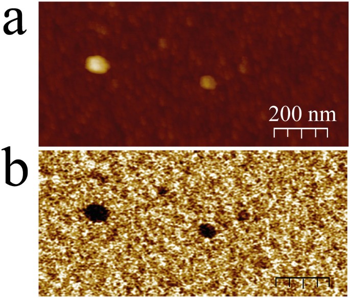
Thin films 120 ± 15 nm thick of Co NPs embedded in TiO2 were obtained by spin coating a water solution of Bis(ammonium lactate)titanium dihydroxide and of cobalt NPs on a Au substrate, the
film was then calcined at high temperature (see detail in methods). As a blank, a thin film of pure TiO2 was prepared following the same procedure.
Besides the occasional formation of large aggregates of NPs, AFM confirms the presence of Co NPs at the solid/air (vacuum) interface. The TiO2 matrix appears to be formed by a homogeneous
distribution of clusters whose mean diameter is