Fabrication of large-area and high-crystallinity photoreduced graphene oxide films via reconstructed two-dimensional multilayer structures
- Select a language for the TTS:
- UK English Female
- UK English Male
- US English Female
- US English Male
- Australian Female
- Australian Male
- Language selected: (auto detect) - EN
Play all audios:
ABSTRACT Graphene, the last representative _sp_2 carbon material to be isolated, acts as an ideal material platform for constructing flexible electronic devices. Exploring a new method to
fabricate high-quality graphene films with high throughput is essential for achieving greater performance with flexible electronic devices. Here, we report a facile coating and subsequent
illumination method for mass-fabricating highly crystalline photoreduced graphene oxide (PRGO) films directly onto conductive substrates. The direct fabrication of PRGO films onto Cu foils
with partial oxygenated groups, an intensive stacked highly crystalline structure, and reduced graphene oxide regions enable significant performance enhancements when used as supercapacitor
electrodes compared with other graphene-only devices, exhibiting high specific capacitances of 275 F g−1 at a scan rate of 10 mV s−1 and 167 F g−1 at 1 V g−1 with excellent rate capability.
The as-established all-solid-state flexible supercapacitors exhibit superior flexibility and robust mechanical stability, resulting in a capacitance delay of only 2% after performing 100
bending cycles. The demonstrated PRGO films provide a promising material platform to realize a broad range of applications related to flexible electronics devices. SIMILAR CONTENT BEING
VIEWED BY OTHERS ENHANCING SUPERCAPACITOR PERFORMANCE THROUGH DESIGN OPTIMIZATION OF LASER-INDUCED GRAPHENE AND MWCNT COATINGS FOR FLEXIBLE AND PORTABLE ENERGY STORAGE Article Open access 30
November 2023 IN SITU FORMATION OF GRAPHENE/METAL OXIDE COMPOSITES FOR HIGH-ENERGY MICROSUPERCAPACITORS Article Open access 17 July 2020 TUNING THE HIERARCHICAL PORE STRUCTURE OF GRAPHENE
OXIDE THROUGH DUAL THERMAL ACTIVATION FOR HIGH-PERFORMANCE SUPERCAPACITOR Article Open access 22 January 2021 INTRODUCTION Flexible electronic devices have garnered considerable attention
because of the benefits enabled by large-area, lightweight, flexible electrode films, which have the potential to enable unique advances in future mobile applications, such as wearable
displays, roll-up solar cells, electronic skin and flexible energy storage.1, 2 Graphene films containing a few layers or multiple layers of two-dimensional graphene sheets are prominent
contenders as attractive components for use in flexible electronic devices due to their high conductivity, chemical stability and mechanical flexibility.3, 4 For the practical applications
of graphene in these fields, scalable production of macroscopic-scale graphene films is required rather than the current micrometer-sized graphene sheets. To date, the synthesis of
large-scale flexible graphene films has mainly been demonstrated by two approaches. One approach is the ‘bottom-up’ synthesis strategy, by which high-quality graphene can be prepared using
chemical vapor deposition to grow graphene at high temperature, followed by a transfer procedure to place graphene films onto flexible substrates;5 however, this method is not sufficiently
cost- and time-effective to be commercially viable for mass production and requires a difficult post-functionalization step to produce the appropriate graphene films. Another approach is the
‘top-down’ method, that is, solution processing of chemically exfoliated graphite, which offer advantages for continuous large-scale production and effective functionalization for
particular applications. Recently, many effective solution-processing methods have been presented, such as spray-coating,6 rod-coating,7 spin-coating,8 the layer-by-layer technique,9 the
Langmuir-Blodgett technique,10 interfacial self-assembly11 and vacuum filtration,12 all of which indicate the feasibility of wet-chemical methods to prepare large-area graphene films,
thereby allowing graphene-based devices to be fabricated on virtually any surface. However, the application of these methods is usually limited by the difficulties in preparing large-area,
high-quality graphene films, which is specifically due to the inefficiency of the homogeneous arrangement of graphene sheets and the appropriate chemical reduction of graphene oxide (GO)
films. These defects hamper the orderly arrangement and effective interlinking of the individual graphene sheets, which results in uncontrollable deep wrinkles and pores in these graphene
films. Therefore, the development of a rapid and low-cost method for preparing flexible, large-scale and high-quality graphene films under mild conditions remains a challenge. Herein, we
report a scalable and solution-processable strategy for assembling GO sheets directly onto conductive substrates (for example, Cu foil) and subsequently reduce the GO sheets into highly
crystalline photoreduced graphene oxide (PRGO) films via a facile illumination treatment. This fabrication method is simple, time-saving and easy to scale up when compared with the
previously reported fabrication techniques for scalable-reduced GO films.7, 13 In this fabrication process, the GO sheets, after derivatization by carboxylic, phenol hydroxyl and epoxide
groups, can readily be exfoliated to form a stable colloidal suspension because they are stabilized by their hydrophilicity and electrostatic repulsion,14, 15 which facilitate the
homogeneous arrangement of GO platelets during the preparation of GO films. The subsequent photoreduction can provide appropriate reduction of the GO films and induce effective interlinking
of the individual graphene sheets. Furthermore, we studied the electrochemical performance of PRGO films that serve as electrode material and observed high specific capacitance and
mechanical flexibility, thus showcasing their potential application in flexible energy storage devices. EXPERIMENTAL PROCEDURES SYNTHESIS OF GRAPHITE OXIDE BY THE HUMMERS METHOD All of the
reagents used were of analytical grade. Ultrapure water (18.2 MΩ resistance) was used in all experiments. Graphite (3.0 g) was added to concentrated H2SO4 (70 ml) under stirring at room
temperature, followed by the addition of NaNO3 (1.5 g) and then the mixture was cooled to 0 °C. Under vigorous agitation, KMnO4 (9.0 g) was added to the solution slowly. After reaction at 35
°C for 2 h, 150 ml of water was added and the solution was then stirred for 15 min at 98 °C. Successively, the solution was diluted with 1:10 HCl aqueous solution (700 ml), followed by a
rapid addition of 400 ml H2O2 (3%). The resulting graphite oxide was isolated and washed by vacuum filtration for further use. PREPARATION OF PRGO FILMS Three steps were followed to prepare
the highly crystalline PRGO films. Preparation of GO gels: in a typical experiment, 5 ml of as-purified graphite oxide suspensions (10 mg ml−1) were dispersed in water (5 ml) to create a
homogeneous dispersion. Exfoliation of graphite oxide to GO was achieved by ultrasonication of the dispersion using a Branson Ultrasonic Cleaner (Branson 3510, 350W, Emerson, St. Louis, MO,
USA) for 1 h and an ultrasonic probe (FS-300, 300W, Sonxi Ultrasonic Instrument, Shanghai, China) for 30 min. The brown dispersion obtained was then subjected to 30 min of centrifugation at
3000 r.p.m. to remove any unexfoliated graphite oxide (usually present in a very small amount) using a centrifuge (5702, Eppendorf, Hamburg, Germany). Next, the GO gels were obtained after
increasing the GO concentration by using a rotary evaporator at 45 °C under∼0.09 MPa for 1 h. Fabrication of GO films: the PRGO films were fabricated by blade coating with an automatic
thick-film coater (AFA-III, MTI Corporation, Richmond, CA, USA). Aliquots (2 ml) of the GO gels were dispensed onto the edge area of a piece of Cu foil, and a scraper was pulled over the
solution at a speed of 15 mm s−1, leaving a uniform wet film that was then dried under ambient conditions. As a control experiment, chemically converted graphene (CCG) films were prepared
using a chemical method to reduce the as-prepared GO films, as reported in previous publications.12 Reduction of the GO films by illumination: reduction of the films was performed under
illumination using a Xe lamp (XQ350-500W, Shanghai Lansheng Electronic Corporation, Shanghai, China) at room temperature for 0.5∼12 h. The PRGO films were cut into the required sizes for
various tests. The weight of the whole piece of film was determined after the film was dried at 100 °C for 12 h. The weight of the films was pre-estimated using the actual area of the films.
The weight was then checked again after testing (after removing the electrolytes by dialysis and drying). If there was any inconsistency, the value obtained by direct weighing of the tested
sample was used. CHARACTERIZATION X-ray diffraction (XRD) spectroscopy was performed using a Rigaku D/max 2550V X-ray diffractometer (D/max 2550V, Rigaku, Tokyo, Japan) using Cu-Kα
irradiation (_λ_=1.5406 Å). The operating voltage and current were maintained at 40 kV and 300 mA, respectively. The morphologies and the structure of the products were characterized using a
high-resolution field emission scanning electron microscope (S-4800, Hitachi, Tokyo, Japan) and a transmission electron microscope (2100F, JEOL, Tokyo, Japan). Atomic force microscopy
images were recorded using a Bruker Dimension 5000 Scanning Probe Microscope in tapping mode (Dimension 5000, Bruker, Camarillo, CA, USA). Raman spectroscopy measurements were performed
using a Renishaw Via laser micro-Raman system (Renishaw, Gloucestershire, UK) at an excitation wavelength of 532 nm. The silicon peak at 520 cm−1 was used as a reference. Fourier transform
infrared (FTIR) spectra were collected using a Thermo Nicolet NEXUS-670 spectrometer (Nicolet NEXUS-670, Thermo Scientific, Waltham, MA, USA). The KBr pellets for FTIR measurements were
prepared by pressing the films and KBr powders using a hand press. The films were supported by transparent polyethylene terephthalate films. X-ray photoelectron spectroscopy measurements
were performed using a Kratos AXIS-ultra spectrometer (AXIS-ultra DLD, Kratos, Manchester, UK) equipped with a monochromatic Al-Kα X-ray radiation source (1486.71 eV). The dielectric
properties of the composite films on fluorine-doped tin oxide-coated glass were measured using a semiconductor device analyzer (E4980A, Agilent, Santa Clara, CA, USA). These measurements
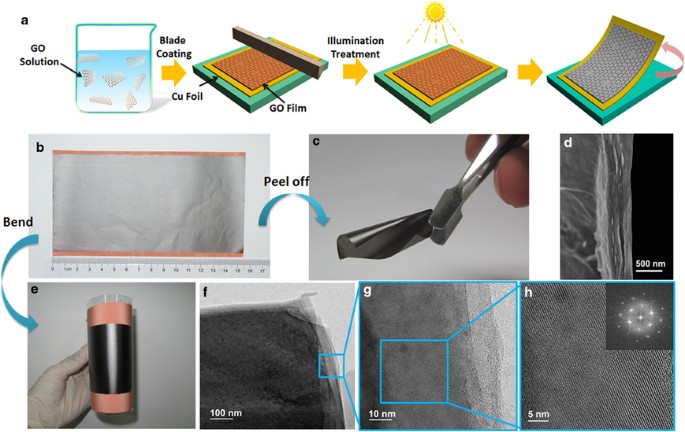
were collected at a voltage of 0.1 V and a frequency of 1 kHz. RESULTS AND DISCUSSION The typical schematic diagram of the fabrication process of PRGO films is shown in Figure 1a. After
ultrasonication and centrifugation treatments, the resulting homogeneous GO solution was concentrated to form stable gels for coating, as shown in Supplementary Figures S1B and S1C.
Subsequently, the PRGO films were deposited onto substrates via blade coating using an automatic thick-film coater. Next, the reduction of the films was performed under illumination at
ambient temperature for different times. Finally, the PRGO films were cut into different sizes for specified measurements or peeled off to yield free-standing PRGO films. Figure 1b shows a
typical image of a PRGO films (8 cm × 15.5 cm), deposited directly onto a Cu foil substrate that was reduced via the illumination treatment performed for 6 h. The PRGO films in contact with
the Cu substrate exhibited a homogeneous shiny graphite luster (Figures 1b, c and e), which indicates the photoreduction of GO to form PRGO and the uniform structure of the fabricated films.
In comparison, the GO films exhibit the characteristic reddish-brown color, thus further demonstrating the formation of PRGO films (Supplementary Figure S1A). Figure 2a schematically
illustrates the microstructural transformation occurring in the fabrication procedure, which was revealed by the atomic force microscopy, scanning electron microscopy and transmission
electron microscopy (TEM) characterizations. The sizes of the GO nanosheets in GO solution are in the range of nanometers to micrometers, with a typical thickness of approximately 1.1 nm
(Supplementary Figure S2). Considering that the thickness of individual GO sheets is approximately 1 nm,16, 17 the GO in this work is one or two layers, indicating the homogeneous dispersion
of GO. However, after PRGO films are formed, the boundary of individual GO nanosheets disappears. Meanwhile, the PRGO film-surface studies (Supplementary Figure S3) clearly indicate that
there are some quasi-one-dimensional creases, which were formed by the overlap of GO sheets due to the folding of the GO edges with neighboring sheets during film fabrication. This result is
also supported by the cross-sectional scanning electron microscopy image of the wavy PRGO films (Supplementary Figure S4), which were immersed into liquid nitrogen and blown by the released
gas. This phenomenon revealed that the edge of one PRGO sheet is entirely in contact with the neighboring sheets and that the sheets are effectively interlinked. To explore the specific
microstructure of the PRGO films, the cross-sectional scanning electron microscopy images of the PRGO films were observed, as shown in Figures 1d and 2b. The morphology exhibits few
microcracks, and interspaces between the layers of the PRGO and the GO films (without illustration reduction) are observed in the cross-section images (Supplementary Figures S5A, B, D, E),
which is different from the incompact structure of CCG films (Supplementary Figures S5C, F, using the reported method12, 18). The well-packed nature of the PRGO sheets was further confirmed
by TEM. Supplementary Figures S6A and S6B show TEM images of the GO films, indicating micrometer-scale wrinkles with a loose GO nanosheet structure. In the high-magnification TEM images of
the GO films (Supplementary Figures S6C and D), lattice fringes were not obvious because of the random arrangement characteristic of GO sheets. In contrast, Figures 1f and g indicate that
the TEM images of PRGO films appear as continuous and tightly stacked edges. In particular, the high-resolution TEM image shown in Figure 1h reveals clear lattice fringes, providing further
definitive evidence for the highly crystalline nature of the PRGO films. The inset in Figure 1h clearly shows the diffraction pattern resulting from performing fast Fourier transformation on
the image of lattice fringes. This hexagonal pattern shows the typical six-fold symmetry expected for graphene,19, 20 which also indicates the high in-plane crystallinity of the PRGO
sheets. As shown in Supplementary Figure S7, the GO films were immediately dissolved into the solution during 30 s of ultrasonication. In contrast, the PRGO films remained almost unchanged
after the same duration of ultrasonication, which further demonstrated the effective reduction of PRGO sheets. XRD analyses also provide structural information for both types of samples
(Figure 2c), particularly focusing on the crystallinity and interlayer distance. The XRD pattern of the exfoliated GO is characterized by a peak at 2_θ_=11.7° with a larger d-spacing of 7.8
Å (compared with the typical value of 3.34 Å in pristine graphite) due to the insertion of hydroxyl and epoxy groups between the carbon sheets and the carboxyl groups along the terminal and
lateral sides of the sheets as a result of the oxidation process of graphite. Following the photoreduction process, the XRD pattern of the PRGO films exhibits a sharp peak centered at
2_θ_=26.4° and a broad low-intensity peak at 2_θ_=23.8°, which is most likely due to both the crystalline domain sizes of the graphitic planes and the nature of the expanded graphene sheets,
which is consistent with previous TEM results. This peak corresponds to 2_θ_=10.7°, with an interlayer spacing of 0.82 nm, which is due to the presence of the remaining oxygen-containing
groups. In combination with the electron microscopy characterization, the good arrangement of the layer-by-layer structure and the intensive connection between the neighboring sheets, which
is induced by photoreduction, is the primary factor that enables the continuous and large-scale manufacturing of PRGO films. To further identify the composition and crystal structure, we
also characterized the PRGO films by means of Raman spectroscopy, X-ray photoelectron spectroscopy and FTIR spectroscopy. The FTIR spectrum (Supplementary Figure S8A) reveals that the
intensity of the characteristic peaks corresponding to oxygen-containing chemical groups decreases dramatically after the photoreduction. The decrease is particularly associated with the
vibration and deformation peaks of O–H groups at 3421 cm−1 and 1400 cm−1, the C=O stretching vibration peak at 1729 cm−1, and the C–O (alkoxy) stretching vibration peak at 1078 cm−1.11 The
X-ray photoelectron spectroscopy technique spectra (Figures 2d–f) were used to investigate the chemical composition and valence states of these films. The broad C1 s peak of the pure GO, CCG
and PRGO films can be fitted into four peaks with binding energies at 284.6, 286.2, 287.8 and 289.0 eV, corresponding to the C–C, C–O, C=O and C(O)O groups, respectively.21 The peak
intensity of the C=O and C–O of the CCG and PRGO films is significantly decreased after photoreduction, which further confirms the successful completion of the reduction process. As seen in
Figure 2f, the residual oxygen-containing chemical groups remaining in the PRGO films are mainly due to the incomplete deoxygenation. The change of the electronic structure in the PRGO
sheets was further explored by Raman spectroscopy (Supplementary Figure S8B). Analogously, after reduction via light, the intensity ratio of the D band (_ca_. 1340 cm−1) to G band (_ca_.
1590 cm−1), the D/G ratio, increased from 0.96 for the pure GO films to 1.12 for the PRGO films, which is still smaller than the value of 1.35 for the CCG films. The spectroscopic
observations thus support the notion that most of the oxygenated groups in the graphitic planes are removed and the _sp_2 planes are largely restored; however, a significant number of
functional groups at the specific area of the nanosheets are most likely retained. Under illumination, the photothermoelectric effect22 should have a key role in this photoreduction process.
The photocurrent induced by the photothermoelectric effect is determined by the photo-induced temperature difference Δ_T_ between the upper surfaces of GO films and the substrate
(Supplementary Figure S9). With the photocurrent between the two surfaces of the film, the deoxygenation occurs within almost the entire GO film. One of the most promising applications of
graphene films is their use as electrode material for supercapacitors due to their large specific surface area, high conductivity and excellent electrochemical stability.2, 23, 24 Recently,
graphene-based macroscopic films have received increasing attention for use in electrochemical energy storage applications.25, 26, 27, 28, 29 Despite these examples of significant progress,
most of the studies of graphene-based films for use in supercapacitors to date involved the fabrication of free-standing graphene films or the preparation of electrodes with the binder first
and then the transfer of the electrode film onto current collector (conductive substrate, for example, platinum, gold or copper foil); such processes introduce high contact resistance
between the electrode and the current collector, which result in significant loss of storage and transmission capacity. Our PRGO films are directly coated onto conductive substrate, which
advantageously minimizes the contact resistance, thus enabling the double-layer charges to be conveniently transferred to the current collector to cause the partial reduction of GO films and
to further enhance the capacitance performance.30 A symmetrical two-electrode system was used to characterize the electrochemical characteristics of the as-fabricated PRGO films in
comparison with those of the GO films and the CCG films. Figure 3a shows the cyclic voltammograms (CVs) of the PRGO films, the GO films and the CCG films in 1 mol l−1 Na2SO4 aqueous
solutions for applied potentials between 0 V and 0.8 V at a scan rate of 50 mV s−1. The CV curves of CCG films exhibit a typical rectangular shape, implying pure electric double-layer
capacitive behavior. In contrast, the CV curves of both GO and PRGO films exhibit a box-like shape superimposed with a well-broadened peak at 0.2–0.6 V, indicating the coexistence of
electric double-layer capacitance and pseudocapacitance. The deviations of the CV curves at specific potential regions are related to the rapid Faradaic reactions, which may be correlated to
the presence of additional oxygen-containing functional groups, especially epoxy and alkoxy, at the surface of the carbon.27, 30 PRGO films exhibit the largest current density in the CV
curves, implying a larger capacitance than those of the GO and CCG films. Figure 3b shows the CV curves of the PRGO films at different scan rates. Even when the scan rate increases to 1000
mV s−1, the CV curve basically maintains the Faradaic peak-incorporated rectangular shape, similar to that observed at 20 mV s−1, which is indicative of the rapid charge-propagation
capability of both the electric double-layer capacitance and the pseudocapacitance in the PRGO electrode. The specific capacitances at different scan rates are calculated based on the CV
measurements. The highest capacitance of 275 F g−1 were achieved for the PRGO films at scan rate of 10 mV s−1, which are exceptionally higher than the values of the GO films (103 F g−1), the
CCG films (146 F g−1) and those reported previously for graphene.23, 28, 31 Furthermore, on increasing the scan rate up to 1000 mV s−1, the specific capacitance remain stable at 167 F g−1,
highlighting the excellent rate capability of PRGO films. We compared the capacitance performances of the PRGO films with those of recent research works focused on graphene-based films for
supercapacitors by examining the data presented in Supplementary Tables S2 and S3. The PRGO films outperform these typical pure CCG-based carbon materials in terms of high capacitance.
Moreover, the performance of PRGO films is even comparable with those of doped or functionalized graphene-based electrodes. Partial oxygen-containing groups on PRGO films were retained
during the photoreduction process, which was confirmed by XRD, FTIR and XPS analysis, as presented above. The partially retained oxygen-containing groups are advantageous, as they can
provide a large additional pseudocapacitance as well as improved wettability, providing PRGO films with a higher capacitance than that of the CCG films. In contrast to the current density of
the PRGO films, the current density in the CV curve of the GO films is not as high, although the content of the oxygen-containing groups in the GO films is notably higher than that in the
PRGO films. The reason that the PRGO films possess a much higher capacitance than the GO electrode is most likely due to the intensively stacked highly crystalline structure of the PRGO
films and the reduced graphene regions, which lead to a dramatic increase in the electrical conductivity along the vertical direction of the electrode. In addition, we believe that the
polarization occurring on the surface of the electrode material could be another important factor for enhanced capacitance. In PRGO films, the neighboring conductive PRGO platelets and
partially reduced PRGO sheets with the remaining oxygen-containing groups in between the sheets could result in interfacial polarization, which leads to internal barrier layer capacitors.32
In general, interfacial polarization can lead to the enhancement of the dielectric constant. Thus, we tested the dielectric constant of different films to confirm the interfacial
polarization influence on the capacitance. The PRGO film exhibited a higher dielectric constant than those of the GO and CCG films (Supplementary Table S1). Therefore, we conclude that the
increase of the dielectric constant induced by interfacial polarization is another key factor for the enhancement the electrochemical performance of PRGO films. To evaluate the influence of
photoreduction on the capacitance of the PRGO films, we performed a detailed study of the impact of the illumination time (0.5–12 h) within a large range of the scan rates on the
capacitance. As shown in Figure 3c, we obtained CV curves of the PRGO films formed using different illumination times ranging from 0.5 to 12 h at a scan rate of 50 mV s−1. The current
response increases with a rise in illumination time at time range from 0.5 to 6 h, indicating an enhancement of the total capacitance. However, with the continued lengthening of the
illumination time, the current density exhibits a slight decrease. The decrease of the specific capacitances with increasing illumination time may due to the additional illumination, leading
to the decrease in the content of oxygen-containing functional groups. The decrease could result in the decrease of pseudocapacitive reactions, as indicated by the weakened peak of the CV
curves. The specific capacitances of PRGO films formed by reduction over different times, GO films and CCG films are plotted in Figure 3d. The specific capacitance of the PRGO films with
illumination of 6 h is higher than those of all other samples, which indicate that the 6-h reduction is the optimal experimental condition for fabricating supercapacitor electrodes. Further
electrochemical investigation was performed to determine the frequency response as well as the equivalent series resistance of the symmetrical two-electrode measurement system based on the
fabricated materials. The electrochemical impedance spectroscopy plots of the PRGO, GO and CCG films are shown in Figures 3e and f. In the low-frequency portion of the spectrum of the PRGO
films and the GO films, both impedance spectra tend toward a vertical line, where the imaginary part of impedance rapidly increases, which is characteristic of capacitive behavior due to the
ion diffusion in the electrode structure. In comparison, the CCG films exhibit an expanded Warburg region, reflecting slow ion transport. The knee frequency is used to evaluate the
frequency dependence of a capacitor and is considered to be the critical frequency at which supercapacitors begin to exhibit capacitive behavior. As shown in Figure 3f, the knee frequency of
the PRGO films is over 660 Hz, indicating that most of its stored energy is accessible at frequencies below 660 Hz, whereas the knee frequencies of the GO and CCG films are much lower, at
265 Hz and 211 Hz, respectively. The knee frequencies of the PRGO films are much higher than some of the reported values for the graphene and carbon nanotube electrodes,33, 34 which could be
the result of rapid electrolyte ions access and diffusion through the conductive paths and the GO sheets. In the high-frequency region, the first intersections of the curves with the real
axis indicate the ohmic resistance _R_0 or the equivalent series resistance, which represents the sum of the resistance of the electrolyte, the intrinsic resistance of the electrode
materials, and the contact resistance between the interfaces of electrode material, electrolyte, and current collector.31 The measured impedance spectra were analyzed based on an equivalent
circuit, which is shown in the inset of Figure 3e. The calculated ohmic resistance _R_0 of the PRGO films and the GO films were estimated to be quite low values of 0.89 Ω and 0.92 Ω,
respectively, in contrast to 2.47 Ω for the CCG films, indicating the well-connected nature of the interfaces of the electrode films, electrolyte ions, and current, due to the intensive
contact between the electrode films and conductive substrate and the improved wettability provided by the oxygen-containing groups. To demonstrate the performance of the fabricated PRGO
electrodes for use in flexible energy storage, we finally assembled all-solid-state flexible supercapacitors using PRGO films as an active electrode material. Figure 4a shows the processing
steps used to fabricate PRGO film-based solid-state flexible supercapacitors. To assemble the solid-state supercapacitor device, H2SO4/polyvinyl alcohol gel was used as the electrolyte,
which would additionally protect the PRGO micropatterned electrodes from wear and breakage due to its excellent mechanical integrity.33 The fabricated device was highly flexible and robust.
The capacitive performance of the flexible solid-state supercapacitors was evaluated by CV (Figure 4b). In general, the shape of the CV loop also exhibits the Faradaic peak-incorporated
rectangular shape, similar to that observed in the previous analysis, which indicates that the capacitance combined both the electric double-layer capacitance and the pseudocapacitance in
the PRGO electrode. The specific capacitance of the graphene hydrogel film electrode estimated from the CV curves was 130 F g−1, which is substantially higher than those of most of the
previously reported solid-state devices made of carbon nanotubes (50–115 F g−1),35, 36 and graphene films (62–120 F g−1).37, 38, 39 A long mechanical stability is an important concern for
practical applications of flexible all-solid-state supercapacitors. To investigate the mechanical stability of as-prepared PRGO all-solid-state supercapacitors, CV cycling tests were
performed at a scan rate of 50 mV s−1 for 100 bending cycles. As shown in Figure 4c, the capacity decay is only 2% of the initial discharge capacity, indicating the excellent mechanical
stability of the PRGO-based all-solid-state supercapacitors. CONCLUSIONS In conclusion, we have fabricated large-scale and flexible films of highly crystalline and intensively stacked
structures directly onto conductive substrates via a facile coating and subsequent illumination method. Through the coating process and photoreduction, GO platelets were reconstructed to
form layer-by-layer-stacked PRGO films. This method has the advantages of being a fast, simple process that is high throughput, and low cost for the preparation of large-area, high-quality
PRGO films directly onto conductive supports or substrates. Compared with previously reported scalable-reduced GO films, PRGO films exhibit greatly improved performance as flexible electrode
materials for supercapacitors. The PRGO films exhibited an 88% increase in specific capacitance compared with that of CCG films, mainly due to the minimized contact resistance and the
additional pseudocapacitance. In addition, the interfacial polarization between the neighboring graphene platelets and the nonconductive GO sheets plays a crucial role in the enhancement of
the capacitance, although the exact chemistry behind this phenomenon requires further study. Because of the scalable synthesis and the demonstrated promising properties, these PRGO films are
promising for use in applications in flexible electronics devices. REFERENCES * Rogers, J. A., Someya, T. & Huang, Y. Materials and mechanics for stretchable electronics. _Science_ 327,
1603–1607 (2010). Article CAS Google Scholar * El-Kady, M. F. & Kaner, R. B. Scalable fabrication of high-power graphene micro-supercapacitors for flexible and on-chip energy
storage. _Nat. Commun._ 4, 1475 (2013). Article Google Scholar * Allen, M. J., Tung, V. C. & Kaner, R. B. Honeycomb carbon: a review of graphene. _Chem. Rev._ 110, 132–145 (2009).
Article Google Scholar * Dai, L. M. Functionalization of graphene for efficient energy conversion and storage. _Acc. Chem. Res._ 46, 31–42 (2012). Article Google Scholar * Zhang, Y.,
Zhang, L. & Zhou, C. Review of chemical vapor deposition of graphene and related applications. _Acc. Chem. Res._ 46, 2329–2339 (2013). Article CAS Google Scholar * Pham, V. H., Cuong,
T. V., Hur, S. H., Shin, E. W. & Kim, J. S. Fast and simple fabrication of a large transparent chemically-converted graphene film by spray-coating. _Carbon. NY_ 48, 1945–1951 (2010).
Article CAS Google Scholar * Wang, J., Liang, M. H., Fang, Y., Qiu, T. F., Zhang, J. & Zhi, L. J. Rod-coating: towards large-area fabrication of uniform reduced graphene oxide films
for flexible touch screens. _Adv. Mater._ 24, 2874–2878 (2012). Article CAS Google Scholar * Becerril, H. A., Mao, J., Liu, Z. F., Stoltenberg, R. M., Bao, Z. N. & Chen, Y. S.
Evaluation of solution-processed reduced graphene oxide films as transparent conductors. _ACS Nano_ 2, 463–470 (2008). Article CAS Google Scholar * Güneş, F., Shin, H. J., Biswas, C. D.,
Han, G. H., Kim, E. S., Chae, S. J., Choi, J. Y. & Lee, Y. H. Layer-by-layer doping of few-layer graphene film. _ACS Nano_ 4, 4595–4600 (2010). Article Google Scholar * Li, X., Zhang,
G. Y., Bai, X. D., Sun, X. M., Wang, X. R., Wang, E. G. & Dai, H. J. Highly conducting graphene sheets and Langmuir-Blodgett films. _Nat. Nanotechnol._ 3, 538–542 (2008). Article CAS
Google Scholar * Gan, S., Zhong, L. J., Wu, T. S., Han, D. X., Zhang, J. D., Ulstrup, J., Chi, Q. J. & Niu, L. Spontaneous and fast growth of large-area graphene nanofilms facilitated
by oil/water interfaces. _Adv. Mater._ 24, 3958–3964 (2012). Article CAS Google Scholar * Li, D., Muller, M. B., Gilje, S., Kaner, R. B. & Wallace, G. G. Processable aqueous
dispersions of graphene nanosheets. _Nat. Nanotechnol._ 3, 101–105 (2008). Article CAS Google Scholar * Cao, X., Qi, D. P., Yin, S. Y., Bu, J., Li, F. J., Goh, C. F., Zhang, S. &
Chen, X. D. Ambient fabrication of large-area graphene films via a synchronous reduction and assembly strategy. _Adv. Mater._ 25, 2957–2962 (2013). Article CAS Google Scholar * Luo, J.,
Kim, J. & Huang, J. Material processing of chemically modified graphene: some challenges and solutions. _Acc. Chem. Res._ 46, 2225–2234 (2013). Article CAS Google Scholar * Raidongia,
K. & Huang, J. Nanofluidic ion transport through reconstructed layered materials. _J. Am. Chem. Soc._ 134, 16528–16531 (2012). Article CAS Google Scholar * Jung, I., Dikin, D. A.,
Piner, R. D. & Ruoff, R. S. Tunable electrical conductivity of individual graphene oxide sheets reduced at ‘low’ temperatures. _Nano Lett._ 8, 4283–4287 (2008). Article CAS Google
Scholar * Eda, G. & Chhowalla, M. Chemically derived graphene oxide: towards large-area thin-film electronics and optoelectronics. _Adv. Mater._ 22, 2392–2415 (2010). Article CAS
Google Scholar * Bai, H., Li, C. & Shi, G. Functional composite materials based on chemically converted graphene. _Adv. Mater._ 23, 1089–1115 (2011). Article CAS Google Scholar *
Hernandez, Y., Nicolosi, V., Lotya, M., Blighe, F. M., Sun, Z. Y., De, S., McGovern, I. T., Holland, B., Byrne, M., Gun'Ko, Y. K., Boland, J. J., Niraj, P., Duesberg, G., Krishnamurthy,
S., Goodhue, R., Hutchison, J., Scardaci, V., Ferrari, A. C. & Coleman, J. N. High-yield production of graphene by liquid-phase exfoliation of graphite. _Nat. Nanotechnol._ 3, 563–568
(2008). Article CAS Google Scholar * Gu, W., Zhang, W., Li, X. M., Zhu, H. W., Wei, J. Q., Li, Z., Shu, Q. K., Wang, C., Wang, U. L., Shen, W. C., Kang, F. Y. & Wu, D. H. Graphene
sheets from worm-like exfoliated graphite. _J. Mater. Chem._ 19, 3367–3369 (2009). Article CAS Google Scholar * Dreyer, D. R., Park, S., Bielawski, C. W. & Ruoff, R. S. The chemistry
of graphene oxide. _Chem. Soc. Rev._ 39, 228–240 (2010). Article CAS Google Scholar * Gabor, N. M., Song, J. C. W., Ma, Q., Nair, N. L., Taychatanapat, T., Watanabe, K., Taniguchi, T.,
Levitov, L. S. & Herrero, P. J. Hot carrier–assisted intrinsic photoresponse in graphene. _Science_ 334, 648–652 (2011). Article CAS Google Scholar * Stoller, M. D., Park, S., Zhu,
Y., An, J. & Ruoff, R. S. Graphene-based ultracapacitors. _Nano Lett._ 8, 3498–3502 (2008). Article CAS Google Scholar * Yang, X., Zhu, J., Qiu, L. & Li, D. Bioinspired effective
prevention of restacking in multilayered graphene films: towards the next generation of high-performance supercapacitors. _Adv. Mater._ 23, 2833–2838 (2011). Article CAS Google Scholar *
Xu, C., Xu, B. H., Gu, Y., Xiong, Z. G., Sun, J. & Zhao, X. S. Graphene-based electrodes for electrochemical energy storage. _Energy Environ. Sci._ 6, 1388–1414 (2013). Article CAS
Google Scholar * Wen, Z., Wang, X. C., Mao, S., Bo, Z., Kim, H. J., Cui, S. M., Lu, G. H., Feng, X. L. & Chen, J. H. Crumpled nitrogen-doped graphene nanosheets with ultrahigh pore
volume for high-performance supercapacitor. _Adv. Mater._ 24, 5610–5616 (2012). Article CAS Google Scholar * Fang, Y., Luo, B., Jia, Y. Y., Li, X. L., Wang, B., Song, Q., Kang, F. Y.
& Zhi, L. J. Renewing functionalized graphene as electrodes for high-performance supercapacitors. _Adv. Mater._ 24, 6348–6355 (2012). Article CAS Google Scholar * Li, Y., Li, Z. &
Shen, P. K. Simultaneous formation of ultrahigh surface area and three-dimensional hierarchical porous graphene-like networks for fast and highly stable supercapacitors. _Adv. Mater._ 25,
2474–2480 (2013). Article CAS Google Scholar * Chen, J., Sheng, K., Luo, P., Li, C. & Shi, G. Graphene hydrogels deposited in nickel foams for high-rate electrochemical capacitors.
_Adv. Mater._ 24, 4569–4573 (2012). Article CAS Google Scholar * Xu, B., Yue, S. F., Sui, Z. Y., Zhang, X. T., Hou, S. S., Cao, G. P. & Yang, Y. S. What is the choice for
supercapacitors: graphene or graphene oxide? _Energy Environ. Sci._ 4, 2826–2830 (2011). Article CAS Google Scholar * Luo, J., Jang, H. D. & Huang, J. Effect of sheet morphology on
the scalability of graphene-based ultracapacitors. _ACS Nano_ 7, 1464–1471 (2013). Article CAS Google Scholar * Kim, J. Y., Lee, W. H., Suk, J. W., Potts, J. R., Chou, H., Kholmanov, I.
N., Piner, R. D., Lee, J., Akinwande, D. & Ruoff, R. S. Chlorination of reduced graphene oxide enhances the dielectric constant of reduced graphene oxide/polymer composites. _Adv.
Mater._ 25, 2308–2313 (2013). Article CAS Google Scholar * Niu, Z., Zhang, L., Liu, L. L., Zhu, B. W., Dong, H. B. & Chen, X. D. All-solid-state flexible ultrathin
micro-supercapacitors based on graphene. _Adv. Mater._ 25, 4035–4042 (2013). Article CAS Google Scholar * Zhang, C., Peng, Z. W., Lin, J., Zhu, Y., Ruan, G. D., Hwang, C. C., Lu, W.,
Hauge, R. H. & Tour, J. M. Splitting of a vertical multiwalled carbon nanotube carpet to a graphene nanoribbon carpet and its use in supercapacitors. _ACS Nano_ 7, 5151–5159 (2013).
Article CAS Google Scholar * Kaempgen, M., Chan, C. K., Ma, J., Cui, Y. & Gruner, G. Printable thin film supercapacitors using single-walled carbon nanotubes. _Nano Lett._ 9,
1872–1876 (2009). Article CAS Google Scholar * Hu, S., Rajamani, R. & Yu, X. Flexible solid-state paper based carbon nanotube supercapacitor. _Appl. Phys. Lett._ 100, 104103–104104
(2012). Article Google Scholar * Choi, B. G., Hong, J., Hong, W. H., Hammond, P. T. & Park, H. Facilitated ion transport in all-solid-state flexible supercapacitors. _ACS Nano_ 5,
7205–7213 (2011). Article CAS Google Scholar * Choi, B. G., Chang, S. J., Kang, H. W., Park, C. P., Kim, H. J., Hong, W. H., Lee, S. G. & Huh, Y. S. High performance of a solid-state
flexible asymmetric supercapacitor based on graphene films. _Nanoscale_ 4, 4983–4988 (2012). Article CAS Google Scholar * Weng, Z., Su, Y., Wang, D. W., Li, F., Du, J. H. & Cheng, H.
M. Graphene–cellulose paper flexible supercapacitors. _Adv. Energy Mater._ 1, 917–922 (2011). Article CAS Google Scholar Download references ACKNOWLEDGEMENTS We gratefully acknowledge the
financial support given by the Natural Science Foundation of China (No. 51172042), the Specialized Research Fund for the Doctoral Program of Higher Education (20110075130001), the Science
and Technology Commission of the Shanghai Municipality (12nm0503900, 13JC1400200), the Program for Professor of Special Appointment (Eastern Scholar) at the Shanghai Institutions of Higher
Learning, the Innovative Research Team in University (IRT1221), the Program of Introducing Talents of Discipline to Universities (No.111-2-04) and Donghua University (CUSF-DH-D-2013009). We
thank Professor Richard Kaner of UCLA for valuable suggestions and helpful discussions. AUTHOR INFORMATION AUTHORS AND AFFILIATIONS * State Key Laboratory for Modification of Chemical Fibers
and Polymer Materials, College of Material Science and Engineering, Donghua University, Shanghai, China Yuanlong Shao, Hongzhi Wang & Qinghong Zhang * Engineering Research Center of
Advanced Glasses Manufacturing Technology, Ministry of Education, Donghua University, Shanghai, China Yaogang Li Authors * Yuanlong Shao View author publications You can also search for this
author inPubMed Google Scholar * Hongzhi Wang View author publications You can also search for this author inPubMed Google Scholar * Qinghong Zhang View author publications You can also
search for this author inPubMed Google Scholar * Yaogang Li View author publications You can also search for this author inPubMed Google Scholar CORRESPONDING AUTHORS Correspondence to
Hongzhi Wang or Yaogang Li. ETHICS DECLARATIONS COMPETING INTERESTS The authors declare no conflict of interest. ADDITIONAL INFORMATION Supplementary Information accompanies the paper on the
NPG Asia Materials website SUPPLEMENTARY INFORMATION SUPPLEMENTARY INFORMATION (DOC 4516 KB) RIGHTS AND PERMISSIONS This work is licensed under a Creative Commons
Attribution-NonCommercial-NoDerivs 3.0 Unported License. The images or other third party material in this article are included in the article’s Creative Commons license, unless indicated
otherwise in the credit line; if the material is not included under the Creative Commons license, users will need to obtain permission from the license holder to reproduce the material. To
view a copy of this license, visit http://creativecommons.org/licenses/by-nc-nd/3.0/ Reprints and permissions ABOUT THIS ARTICLE CITE THIS ARTICLE Shao, Y., Wang, H., Zhang, Q. _et al._
Fabrication of large-area and high-crystallinity photoreduced graphene oxide films via reconstructed two-dimensional multilayer structures. _NPG Asia Mater_ 6, e119 (2014).
https://doi.org/10.1038/am.2014.59 Download citation * Received: 14 November 2013 * Revised: 09 May 2014 * Accepted: 01 June 2014 * Published: 15 August 2014 * Issue Date: August 2014 * DOI:
https://doi.org/10.1038/am.2014.59 SHARE THIS ARTICLE Anyone you share the following link with will be able to read this content: Get shareable link Sorry, a shareable link is not currently
available for this article. Copy to clipboard Provided by the Springer Nature SharedIt content-sharing initiative